
Method of making a picoscopic scale/ nanoscopic scale circuit pattern

a circuit pattern and picoscopic scale technology, applied in the field of fine circuit pattern making, can solve the problems of increasing the complexity of the manufacturing process of ics, increasing the difficulty of the process and overall production cost, and approaching the technological and economic limit of conventional optical lithography

Pending Publication Date: 2022-07-21
LONGSERVING TECH CO LTD
View PDF0 Cites 0 Cited by
  • Summary
  • Abstract
  • Description
  • Claims
  • Application Information

AI Technical Summary

Benefits of technology

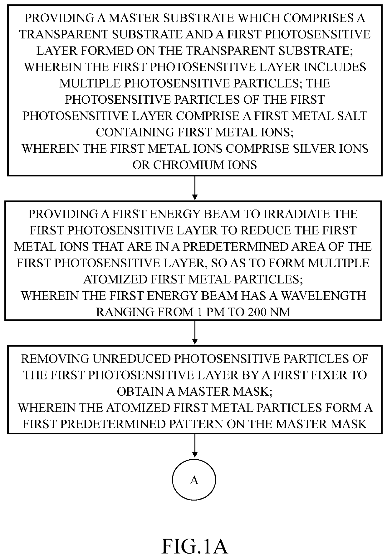
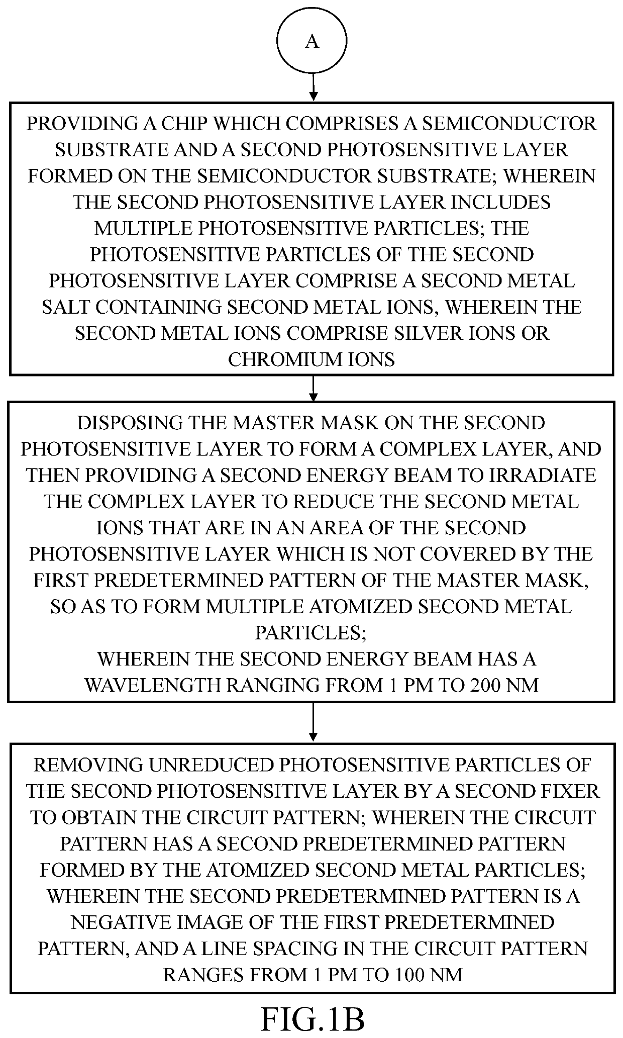
The patent text describes a new method of making circuit patterns for IC manufacturing that overcomes technical problems in conventional processes. This method uses a master mask made of a transparent substrate and a photosensitive layer to directly depict the desired circuit pattern onto the substrate. This obviates the need for a traditional photomask, which is a time-consuming and costly process. The method is also more efficient than current photolithography techniques, allowing for finer lines in the circuit pattern. Additionally, the method can make use of a photosensitizer to enhance sensitivity and accelerate the reduction reaction. The method is simple and cost-effective, and can offer potential for commercial implementation.

Problems solved by technology

Such scaling down process not only increases the complexity of manufacturing process of ICs, but also substantially increases the difficulty of the process and overall production costs.
However, the conventional optical lithography is approaching its technological and economic limit, and ArF laser cannot support the IC chip fabrication with feature size of less than 7 nm, such as 5 nm.
However, when EUV is actually applied to mass production for semiconductor manufacture, innumerable problems need to be overcome.
The most difficult one is how to generate a stable light source with sufficient intensity; in addition, EUV lithography demands a rigorous standard for environmental cleanliness.
Further, EUV lithography is expensive and consumes tremendous amount of electric power.
Accordingly, IC production cost will rise sharply.

Method used


Image

  • Method of making a picoscopic scale/ nanoscopic scale circuit pattern
  • Method of making a picoscopic scale/ nanoscopic scale circuit pattern

Examples


example 1

Method of Making a Circuit Pattern at a Nanoscopic Scale

[0035]Preparing a Master Mask

[0036]First, a master substrate was provided. The master substrate comprised a transparent substrate and a first photosensitive layer formed on the transparent substrate; wherein the first photosensitive layer included multiple photosensitive particles; the photosensitive particles of the first photosensitive layer comprised AgBr particles as the first metal salt containing silver ions. The first photosensitive layer had an average thickness of about 70 nm, and the average particle size of the AgBr particles of the first photosensitive layer was about 50 nm.

[0037]Then, under an environment with a vacuum degree of 10−4 Pa, a first energy beam connecting with a computer system was provided. The computer system operated the emission of the first energy beam, so the first energy beam could directly depict a negative image of a desired IC pattern onto the first photosensitive layer. Accordingly, AgBr par...

example 2

Method of Making a Circuit Pattern at a Picoscopic Scale

[0045]Preparing a Master Mask

[0046]First, a master substrate was provided. The master substrate comprised a transparent substrate and a first photosensitive layer formed on the transparent substrate; wherein the first photosensitive layer included multiple photosensitive particles; the photosensitive particles of the first photosensitive layer comprised AgBr particles as the first metal salt containing silver ions. The first photosensitive layer had an average thickness of about 50 nm, and the average particle size of the AgBr particles of the first photosensitive layer was about 5 nm.

[0047]Then, under an environment with a vacuum degree of 10−7 Pa, a first energy beam connecting with a computer system was provided. The computer system operated the emission of the first energy beam, so the first energy beam could directly depict a negative image of a desired IC pattern onto the first photosensitive layer. Accordingly, AgBr part...


PUM

PropertyMeasurementUnit
wavelengthaaaaaaaaaa
particle sizeaaaaaaaaaa
sizeaaaaaaaaaa

Abstract

Provided is a method of making a circuit pattern. The method includes: Step (A): providing a master substrate comprising a first photosensitive layer containing photosensitive particles; Step (B): providing an energy beam to reduce metal ions in a predetermined area of the first photosensitive layer to form multiple first metal particles; Step (C): removing unreduced photosensitive particles by a fixer to obtain a master mask; wherein the first metal particles form a first predetermined pattern in the master mask; Step (D): providing a chip comprising a second photosensitive layer containing second photosensitive particles; Step (E): putting the master mask on the second photosensitive layer and providing an energy beam to reduce metal ions of an uncovered part of the second photosensitive layer to form multiple atomized second metal particles; Step (F): removing unreduced photosensitive particles by a fixer to obtain the circuit pattern having line spacing at picoscopic / nanoscopic scale.

Description

CROSS-REFERENCE TO RELATED APPLICATION[0001]Pursuant to 35 U.S.C. § 119(a), this application claims the benefit of the priority to Taiwan Patent Application No. 110101810, filed on Jan. 18, 2021. The content of the prior application is incorporated herein by its entirety.BACKGROUND OF THE INVENTION1. Field of the Invention[0002]The present disclosure relates to a method of making a circuit pattern, and more particular to a method of making a fine circuit pattern for integrated circuits.2. Description of the Prior Arts[0003]For nearly 6 decades, the invention of chips composed of semiconductor integrated circuits (ICs) has driven the global technological development in leaps and bounds and has hugely changed human life. With ihe increasing demand for small, lightweight and high-performing electronic and electrical products, the functional density of ICs needs to be generally increased while the geometric size of ICs needs to be generally decreased. Such scaling down process not only ...

Claims


Application Information

Patent Timeline
Patent Type & Authority Applications(United States)
IPC IPC(8): G03F7/004G03F7/20G03F7/32H01L21/027
CPCG03F7/0043H01L21/0275G03F7/325G03F7/2006G03F7/2014G03F7/2047G03F7/0042G03F7/7035G03F1/50H01L21/0274G03F7/2004G03F7/3092G03F7/32
Inventor FANG, KO-CHENG
Owner LONGSERVING TECH CO LTD
Learn More