Flexible electronic element substrate, organic thin film solar cell, laminated structure and method for manufacturing the same, and method for manufacturing flexible electronic element

a technology of electronic elements and substrates, applied in the direction of final product manufacturing, sustainable manufacturing/processing, synthetic resin layered products, etc., can solve the problems of low flexibility, easy cracking of glass substrates, and needing careful handling, and achieve high visible light transmittance, suppress deterioration, and low ultraviolet light transmittance

Pending Publication Date: 2021-10-21
RIKEN +1
View PDF4 Cites 0 Cited by
  • Summary
  • Abstract
  • Description
  • Claims
  • Application Information

AI Technical Summary

Benefits of technology

[0043]Present invention provides a substrate for a flexible electronic device including a polyimide layer having both a low ultraviolet light transmittance and a high visible light transmittance and capable of suppressing deterioration due to the ultraviolet light exposure without deteriorating performance of the electronic device.

Problems solved by technology

However, the glass substrate is easily cracked and require careful handling, and they have the disadvantage of low flexibility.

Method used


Image

  • Flexible electronic element substrate, organic thin film solar cell, laminated structure and method for manufacturing the same, and method for manufacturing flexible electronic element
  • Flexible electronic element substrate, organic thin film solar cell, laminated structure and method for manufacturing the same, and method for manufacturing flexible electronic element
  • Flexible electronic element substrate, organic thin film solar cell, laminated structure and method for manufacturing the same, and method for manufacturing flexible electronic element

Examples


example 1

[0157](Forming Fluorine-Based Resin Layer)

[0158]200 μl of fluorine-based resin layer composition obtained by mixing a fluorine-based coating agent 1 (manufactured by 3M Co., Ltd., NOVEC 270) and a fluorine-based coating agent 2 (manufactured by 3M Co., Ltd., NOVEC200) at a mass ratio of 1:1 was dropped onto a peeling substrate made of an inorganic glass plate (alkali glass, 0.7 mm thickness), and spin-coated. The spin coating conditions were 1000 rpm for 60 seconds. Thereafter, the laminate was left at room temperature for 3 minutes to form a fluorine-based resin layer having a thickness of 100 nm on the inorganic glass plate. The surface of the obtained fluorine-based resin layer was subjected to an oxygen plasma treatment. The plasma treatment was carried out for 30 seconds at an oxygen-gas flow rate of 5 sccm and a power of 50 W using PC300 manufactured by SAMCO Co. Ltd.

[0159](Forming Polyimide Substrate (Device Substrate))

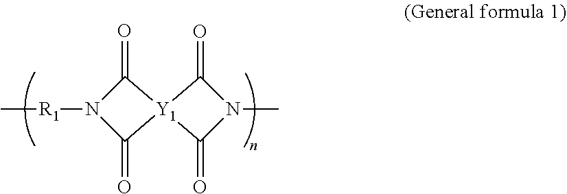
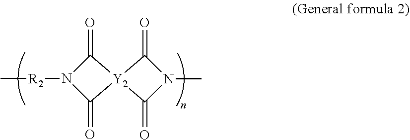
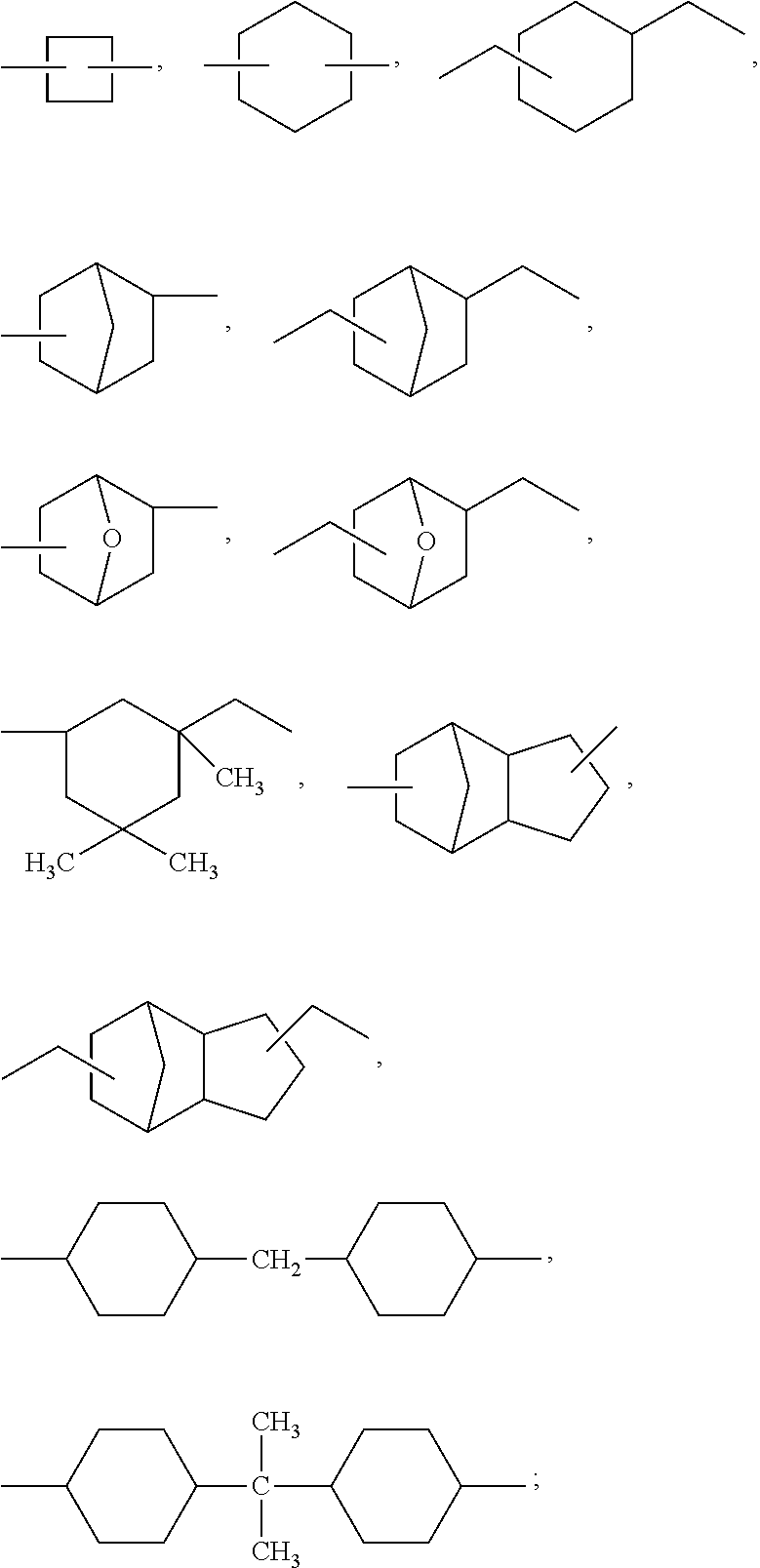
[0160]5.71 g (0.05 mol) of 1,4-diaminocyclohexane (CHDA),...

example 2

[0186]In the same manner as in the method for manufacturing the laminated structure described above, a fluorine-based resin layer was formed on the inorganic glass substrate (peeling substrate), and the polyimide substrate (thickness: 1.2 μm) was further formed. The physical properties of the obtained polyimide substrate are the same as the values shown in Table 1 described above.

[0187]An indium tin oxide (ITO) layer was formed on the polyimide substrate of the laminated structure by sputtering method. The thickness of the ITO layer (first electrode) was 100 nm. The obtained ITO layer was subjected to oxygen plasma treatment for 1 minute at an oxygen gas flow rate 5 sccm and the power of 300 W by PC300 manufactured by SAMCO Co., Ltd.

[0188]Subsequently, a solution obtained by dissolving 549 mg of zinc acetate dihydrate and 160 μl of ethanolamine in 5 ml of 2-methoxyethanol was added dropwise onto the ITO layer and spin-coated. The spin coating conditions were 5,000 rpm for 30 seconds...


PUM

PropertyMeasurementUnit
transmittanceaaaaaaaaaa
thicknessaaaaaaaaaa
thicknessaaaaaaaaaa

Abstract

The present invention addresses the problem of providing a flexible electronic element substrate comprising a polyimide layer that has both low ultraviolet transmittance and high visible light transmittance and that is capable of suppressing ultraviolet degradation without any reduction in the performance of an electronic element. In order to solve this problem, the flexible electronic element substrate comprises a polyimide layer that satisfies all of (1) through (3) below: (1) maximum transmittance at a wavelength of 400±5 nm is 70% or higher at a thickness of 5 μm; (2) the b* value in an L*a*b* color system is 5 or less at a thickness of 5 μm; and (3) transmittance of light at a wavelength of 350 nm is 10% or less at a thickness of 5 μm.

Description

TECHNICAL FIELD[0001]The present invention relates to a substrate for a flexible electronic device, an organic thin film solar cell, a laminated structure and a method for manufacturing the same, and a method for manufacturing a flexible electronic device.BACKGROUND ART[0002]In recent years, electronic devices having flexibility (hereinafter also referred to as “flexible electronic devices”) have been receiving attention. In particular, elements composed mainly of organic materials are receiving attention because of their potential for weight reduction and cost reduction. Especially, organic thin film solar cells are expected to be commercialized.[0003]Conventionally, glass substrates have been mainly used as substrates for thin film solar cells. However, the glass substrate is easily cracked and require careful handling, and they have the disadvantage of low flexibility. Therefore, it has been considered to replace the glass substrate with a substrate composed of a flexible resin.[...

Claims


Application Information

Patent Timeline
Patent Type & Authority Applications(United States)
IPC IPC(8): H01L51/00H01L51/44C08G73/10C08J5/18B05D3/12B05D5/06
CPCH01L51/0097H01L51/44C08G73/10C08J5/18B05D2505/50B05D5/06B05D2203/35B05D2350/60B05D3/12B32B27/34Y02E10/549Y02P70/50C08G73/1042C08G73/1053C08G73/1082H10K77/111H10K30/80B32B27/281B32B27/304B32B2457/12
Inventor FUKUDA, KENJIROKIMURA, HIROKISOMEYA, TAKAOFUKUKAWA, KENICHIOKAZAKI, MASAKIURAKAMI, TATSUHIRO
Owner RIKEN
Why Eureka
Try Eureka