Precise Alignment and Decal Bonding of a Pattern of Solder Preforms to a Surface

a technology of precision alignment and decal bonding, which is applied in the direction of soldering apparatus, semiconductor/solid-state device details, manufacturing tools, etc., can solve the problems of limiting the processing speed of pick-and-place systems, slow manual placement, and affecting the accuracy of solder pattern placement, etc., to achieve high spatial accuracy, high precision, and high placement accuracy

Inactive Publication Date: 2019-06-20
UNITED STATES OF AMERICA
View PDF3 Cites 2 Cited by
  • Summary
  • Abstract
  • Description
  • Claims
  • Application Information

AI Technical Summary

Benefits of technology

[0017]This new process described herein is an efficient and scalable method for bonding electrical circuit patterns at specific locations between an upper and lower surface. The pattern of solder preforms is fabricated on a release tape and has indexed alignment holes at prescribed locations. This indexed tape design allows simple integration into a reel-to-reel system for commercial applications. This method is especially applicable to solder bonding the overlay of filaments from upper and lower high-temperature superconducting (HTS) tapes. This method can also be generalized to allow parallel solder bonding of microscopic features at precise locations between any two overlaid adjacent surfaces.
[0026]The keys to ensuring high placement accuracy of the solder pattern onto a receiving surface are: 1) to fabricate indexing holes in both the release tape containing the solder preforms and the receiving surface(s) and 2) to fabricate the ‘complementary’ indexing pins on an alignment jig. The alignment jig is a device or structure that helps align and assemble all the separate components together on a 2-D planar or 3-D curved surface with high precision. With judicious choice of indexing holes and pins, individual components are aligned to less than 50 microns spatial tolerance. Other methods of indexing components such as mechanical means (e.g. notches, holes, guides) or optical means (e.g. laser, LED, lamp) can be used. As long as there is a ‘complementary’ structure on the alignment jig to match the indexed component, then high spatial accuracy can be maintained.

Problems solved by technology

Manual placement is slow and pick-and-place systems cannot handle very small and fragile components (limited to a few hundred microns thickness).
Although high-speed multiple-head pick-and-place machines exist, the increasing complexity and density of circuitry require ever decreasing solder preform size with wider variety, demands that go beyond the capabilities of current pick-and-place machines.
Ultimately, both prior art methods place the solder preforms in their final locations in a serial manner which limits their processing speeds.
Although both these prior art methods can process solder preforms simultaneously, they cannot be easily implemented in a roll-to-roll environment used for manufacturing tapes.
One problem associated with stamping is the curvature of the surface of the preform caused by the forces acting on it during the stamping process.
The curved surface may reduce the seal between the preform and the vacuum nozzle in an SMT machine resulting in less reliable pick-up and release of the preform.
However the solder preforms were cut individually and not aligned to any pre-defined pattern in a receiving surface.
In these prior art techniques, the shape and size of each solder preform is usually fixed for the entire receiving pattern and not easily changed without redesigning and refabricating the recessed holder.
Irregularly shaped and very thin (<0.25 mm) solder preforms that may be required for highly specialized applications may not be easily handled by current techniques.
Very thin (<0.2 mm thick) and low mass solder preforms are required for fine electronics circuitry (such as high-temperature superconducting (HTS) tapes or foils) and placing them on a receiving sample with high precision (

Method used


Image

  • Precise Alignment and Decal Bonding of a Pattern of Solder Preforms to a Surface
  • Precise Alignment and Decal Bonding of a Pattern of Solder Preforms to a Surface

Examples


example 1

Decal Imprinting and Bonding of Solder (DIBS)

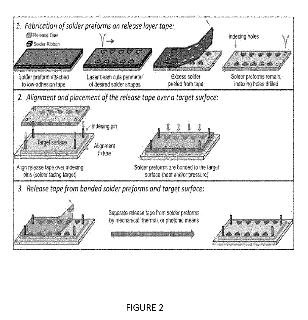
[0032]This invention, which can be termed “Decal Imprinting and Bonding of Solder” (DIBS) consists of three steps—the fabrication of the solder preforms (shape and spacing) on the release (layer or) tape, the alignment and placement of the release tape over a target surface, and release of the individual solder preforms from the release tape onto the target surface and their subsequent bonding to the target surface.

[0033]The solder preforms can be detached from the release tape and bonded to the target surface by mechanical, thermal or photonic means.

example 2

[0034]To fabricate the solder release tape, a strip of semiconductor dicing tape, such as ‘low-tack blue’ is used as the support structure for the solder preforms. Components attached to low tack blue' dicing tape can be removed mechanically. Other types of dicing tape can use heat (Nitto “Revalpha”) or UV light (DU-300) to lower its adhesion properties in order to release its attached components.

[0035]A strip of dicing or release tape about the same size and shape as the target surface is secured to a stable surface, for example a vacuum chuck.

[0036]Next, a ribbon of solder of fixed thickness (e.g. Indium Bismuth eutectic) is pressed onto the release tape.

[0037]A UV (λ=355 nm) laser is then focused onto the solder and perforates the perimeter or outline of the desired solder preforms without damaging the underlying release tape.

[0038]To ensure precise alignment of the release tape (and the solder preforms) to the target surface, the same laser is used to drill indexing holes into t...

example 3

[0040]This solder preform tape can now be guided over the corresponding indexing pins of an alignment jig, which holds the receiving surface, and the solder side placed over and pressed onto receiving surface.

[0041]Solder preforms such as In2Bi, can be mechanically released from the dicing tape and pressure and thermally treated to bond to a compatible surface in a single step.

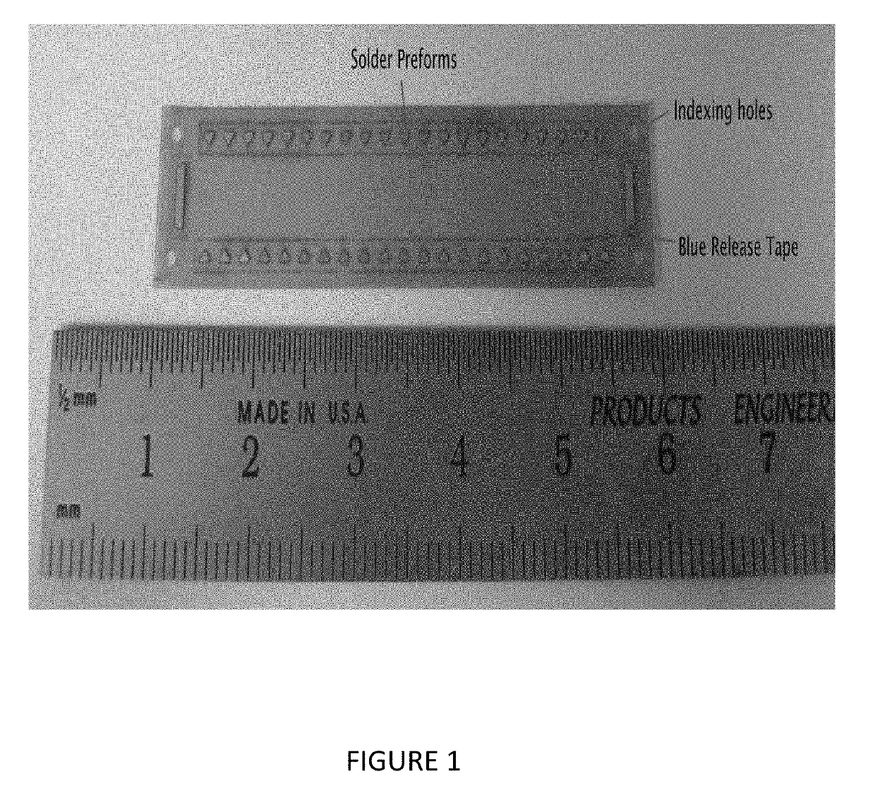
[0042]The release tape can then be removed leaving behind a precisely spaced pattern of solder preforms on the target surface. Note that additional layers or tapes with the same pattern of indexing holes can now be precisely aligned and placed over this first layer of solder preforms. FIG. 1 shows a finished blue ‘low tack’ release tape with a set of solder preforms ready for use.

[0043]This invention enables multiple solder preforms of arbitrary size and shape to be fabricated at precise locations on a release tape. This prescribed pattern of solder preforms matches the location of the corresponding “bond pads...


PUM

PropertyMeasurementUnit
thicknessaaaaaaaaaa
thickaaaaaaaaaa
thicknessaaaaaaaaaa

Abstract

A method of making precise alignment and decal bonding of a pattern of solder preforms to a surface comprising cutting and placing a length of a solder ribbon onto a semiconductor release tape forming a solder ribbon and semiconductor release tape combination, placing the solder ribbon and semiconductor release tape combination on a vacuum chuck on X-Y stage pair in a laser micromachining system, adjusting the working distance, laser-cutting an outline, peeling off the solder ribbon, allowing the desired solder shape to remain, creating indexing holes, providing a target surface on an alignment fixture with indexing pins, aligning the indexing holes, placing the semiconductor release tape with the desired solder shape on the target surface, pressing the desired solder shape onto the target surface, removing the release tape, and making a pattern of the desired solder shape with precise alignment and decal bonding on the target surface.

Description

REFERENCE TO RELATED APPLICATION[0001]This application is a non-provisional of, and claims priority to and the benefits of, U.S. Provisional Patent Application No. 62 / 598,541 filed on Dec. 14, 2017 and U.S. Provisional Patent Application No. 62 / 598,539 filed on Dec. 14, 2017 and U.S. Provisional Patent Application No. 62 / 728,650 filed on Sep. 07, 2018, the entireties of each are hereby incorporated by reference.BACKGROUND[0002]This disclosure concerns precise alignment and decal bonding of a pattern of solder preforms to a surface. The terms ‘surface’ and ‘sample’, ‘receiving’ and ‘target’ will be used interchangeably in this invention.[0003]With the increasing density and complexity of circuitry in modern microelectronics, there is a need to apply solder for attaching components in small precise amounts with tight spatial tolerances.[0004]Solder preforms are precisely formed elements of solder available commercially in various sizes, shapes, thickness and compositions (with or with...

Claims


Application Information

Patent Timeline
Patent Type & Authority Applications(United States)
IPC IPC(8): B23K3/06H01L21/683H01L21/68H01L21/67H01L23/00H01L39/24B23K1/00B23K35/02
CPCH01L24/03H01L21/67092B23K1/0016B23K35/0222H01L2224/03003H01L2224/0311H01L2221/68309H01L2224/05109H01L2224/05113H01L2924/01322H01L2924/014B23K2101/42H01L21/6836B23K3/0623B23K35/264H01L21/6838H01L21/681H01L39/24Y02P80/30H05K3/3478H05K2203/107H05K2203/167H05K2203/1545H05K2203/0531H10N60/203H10N60/0801Y02E40/60H01B12/06H01B13/0036H10N60/0688H10N60/01
Inventor AUYEUNG, RAYMOND C.Y.PRESTIGIACOMO, JOSEPH C.OSOFSKY, MICHAEL S.
Owner UNITED STATES OF AMERICA
Why Eureka
Try Eureka