Metallic and semiconducting carbon nanotube sorting

a carbon nanotube and semiconducting technology, applied in the field of nanomaterial sorting, can solve the problems of low yield or high cost, not readily scalable, low yield, etc., and achieve the effect of reducing detection requirements, fast and efficient sorting, and improving efficiency and scalabl

Active Publication Date: 2014-12-23
EASTMAN KODAK CO
View PDF6 Cites 1 Cited by
  • Summary
  • Abstract
  • Description
  • Claims
  • Application Information

AI Technical Summary

Benefits of technology

[0009]According to one aspect of the invention, separation of semiconducting and metallic nanotubes using a continuous inkjet system that includes electrostatic deflection is provided. Ionic side-groups are selectively attached on metallic nanotubes and concentrated in a drop that can be deflected using a deflection electrode of an electrostatic deflection mechanism. The present invention provides a fast and efficient way to sort metallic and semiconducting nanotubes. When compared to conventional techniques, the present invention reduces the need for detection and does not require a single file stream of nanotubes, thus making the present invention more efficient and scalable.
[0010]One example embodiment of the present invention provides a system and method for separating metallic SWNTs from semiconducting SWNTs or vice versa to obtain a purified batch of semiconducting SWNTs or metallic SWNTs that has higher yield of the desired product, and is more efficient and scalable when compared to conventions systems and methods. The method includes selectively functionalizing metallic SWNTs with charged functional groups in a mixture containing metallic and semiconducting SWNTs such that the metallic SWNTs carry a net charge and forming a dispersion of this mixture in a fluid such that the metallic and semiconducting SWNTs are suspended in this fluid in a stable dispersion. The metallic SWNTs are enriched by sending the mixture through an inkjet printing system and applying an electric field to selectively attract functionalized metallic SWNTs in a drop. The drop enriched with functionalized metallic SWNTs is the separated from other drops, for example, by deflecting the drop using a deflection mechanism. In another embodiment of the present invention, semiconducting SWNTs are functionalized to have a net charge, are enriched, and then separated from other drops.

Problems solved by technology

However, these methods suffer from problems including low yield or high cost.
Each of these techniques, however, is disadvantaged in that they are not readily scalable, suffer from low yield, or are expensive.

Method used


Image

  • Metallic and semiconducting carbon nanotube sorting
  • Metallic and semiconducting carbon nanotube sorting
  • Metallic and semiconducting carbon nanotube sorting

Examples


Embodiment Construction

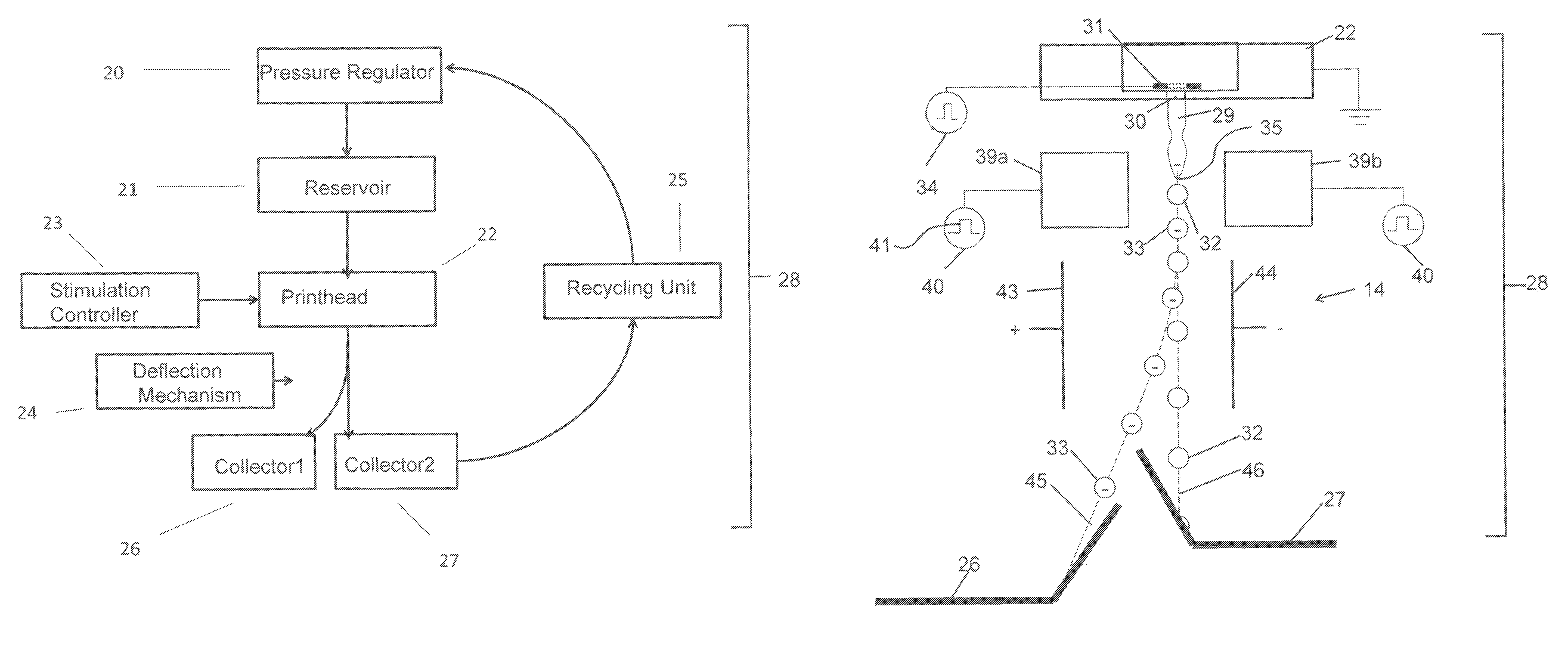
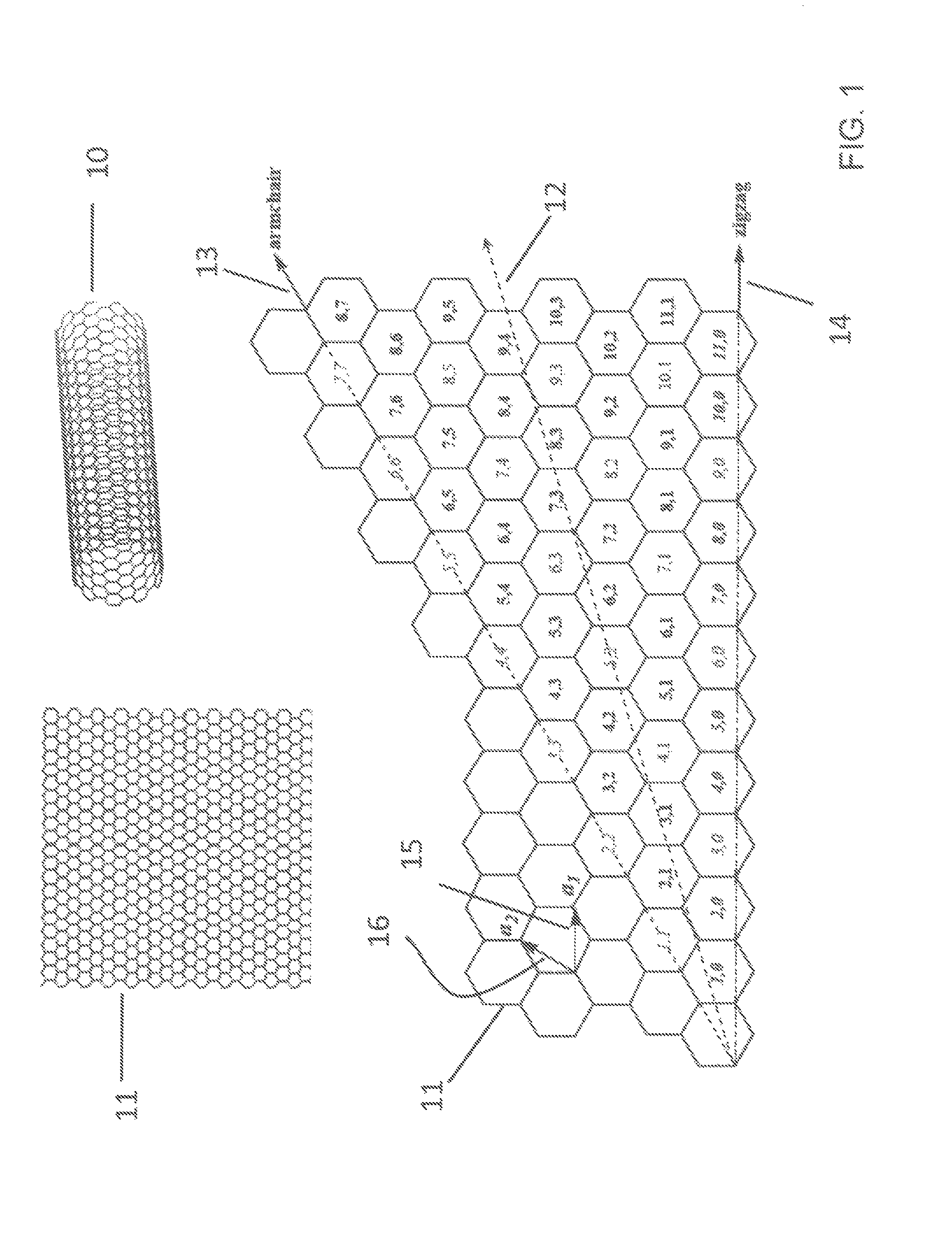
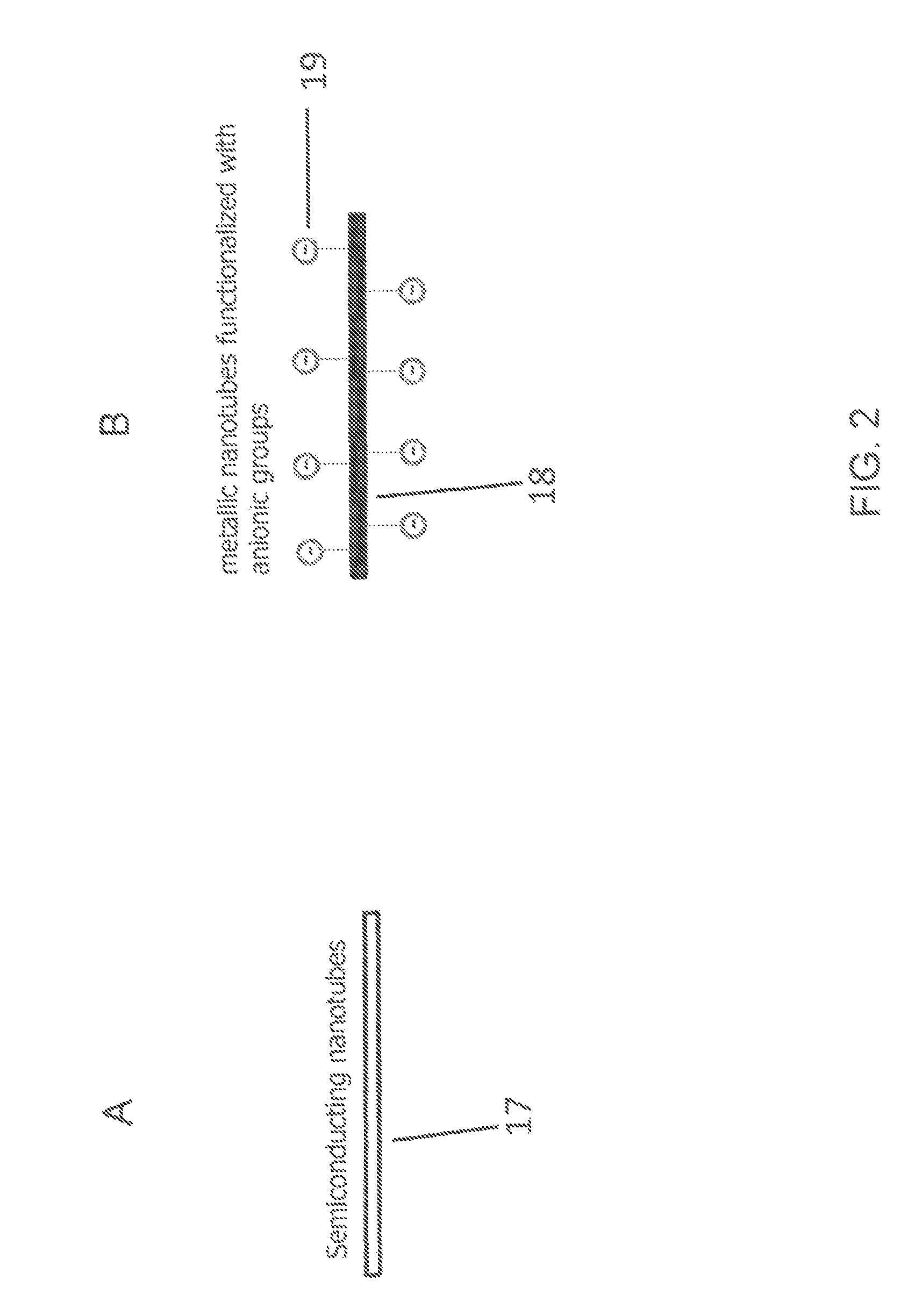
[0020]The present description will be directed in particular to elements forming part of, or cooperating more directly with, apparatus in accordance with the present invention. It is to be understood that elements not specifically shown or described may take various forms well known to those skilled in the art. In the following description and drawings, identical reference numerals have been used, where possible, to designate identical elements.

[0021]The example embodiments of the present invention are illustrated schematically and not to scale for the sake of clarity. One of the ordinary skills in the art will be able to readily determine the specific size and interconnections of the elements of the example embodiments of the present invention.

[0022]Throughout the specification and claims, the following terms take the meanings explicitly associated herein, unless the context clearly dictates otherwise. The meaning of “a,”“an,” and “the” includes plural reference, the meaning of “in...


PUM

PropertyMeasurementUnit
semiconductingaaaaaaaaaa
metallicaaaaaaaaaa
electrostatic forceaaaaaaaaaa

Abstract

A method of printing an electronic device includes providing a source of a mixture of semiconducting carbon nanotubes and metallic carbon nanotubes in a carrier liquid, a printhead, and a substrate. The mixture of semiconducting carbon nanotubes and metallic carbon nanotubes in the carrier liquid is separated using the printhead. One of the separated semiconducting carbon nanotubes and the separated metallic carbon nanotubes is caused to contact the substrate in predetermined pattern.

Description

CROSS REFERENCE TO RELATED APPLICATIONS[0001]Reference is made to commonly-assigned, U.S. patent application Ser. No. 13 / 798,445, entitled “METALLIC AND SEMICONDUCTING CARBON NANOTUBE SORTING”, filed concurrently herewith.FIELD OF THE INVENTION[0002]This invention relates generally to sorting of nanomaterials, and in particularly to separating semiconducting carbon nanotubes and metallic carbon nanotubes.BACKGROUND OF THE INVENTION[0003]A single-wall carbon nanotube (SWNT) is a cylindrical structure formed by rolling up a graphene sheet. The direction and magnitude of the rolling vector define the chirality and diameter, respectively, of the resulting nanotube and determine whether the nanotube is metallic or semiconducting. Common methods used to synthesize SWNT produce complex mixtures that contain many chiralities. Statistically, one third of the mixture is metallic while the remaining mixture is semiconducting. However, many applications of SWNTs, such as conductive films and hi...

Claims


Application Information

Patent Timeline
Patent Type & Authority Patents(United States)
IPC IPC(8): H01L21/00H01L51/00
CPCY10S977/845H01L51/0005H01L51/0049H10K71/135H10K85/225
Inventor ADIGA, SHASHISHEKAR P.PANCHAWAGH, HRISHIKESH V.MARCUS, MICHAEL A.
Owner EASTMAN KODAK CO
Why Eureka
Try Eureka