Method and system for growth of graphene nanostripes by plasma enhanced chemical vapor deposition

a graphene nanostripe and chemical vapor deposition technology, applied in the direction of graphene nanoribbons, chemical vapor deposition coatings, coatings, etc., can solve the problems of incompatibility of device fabrication and integration, need for multiple steps, and inability to meet the requirements of many applications, etc., to achieve enhanced chemical vapor deposition, high yield, and high aspect ratio

Active Publication Date: 2019-03-28
CALIFORNIA INST OF TECH
View PDF0 Cites 9 Cited by
  • Summary
  • Abstract
  • Description
  • Claims
  • Application Information

AI Technical Summary

Benefits of technology

The present invention provides a new method for growing graphene nanostripes using a single-step process without the need for active heating. This method involves the use of substituted aromatics as precursors and low plasma power. The resulting nanostripes have high yields and are of high quality with high aspect ratios and electrical conductivity. This method can be used for various applications such as energy storage, photovoltaic energy harvesting, and conducting composite materials. Compared to conventional thermal CVD processes, the present invention increases manufacturing throughput and enables the growth of high aspect ratio nanostripes with high production yields and high electrical mobility.

Problems solved by technology

However, graphene produced in this manner is not suitable for many applications due to its inherently small size and the non-scalability of the process.
However, the need for multiple steps and high temperatures (˜1000° C.) is incompatible with device fabrication and integration.

Method used


Image

  • Method and system for growth of graphene nanostripes by plasma enhanced chemical vapor deposition
  • Method and system for growth of graphene nanostripes by plasma enhanced chemical vapor deposition
  • Method and system for growth of graphene nanostripes by plasma enhanced chemical vapor deposition

Examples


Embodiment Construction

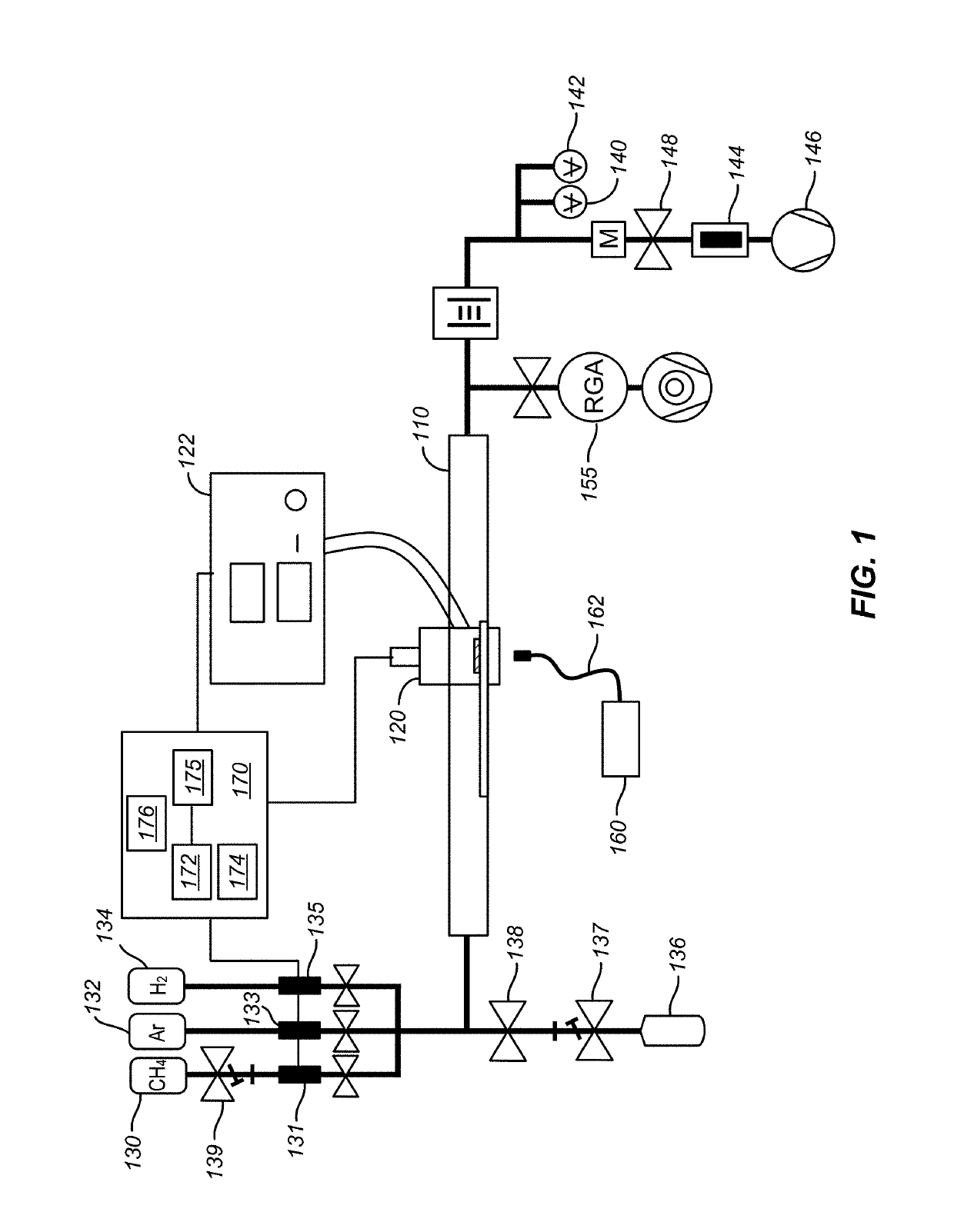
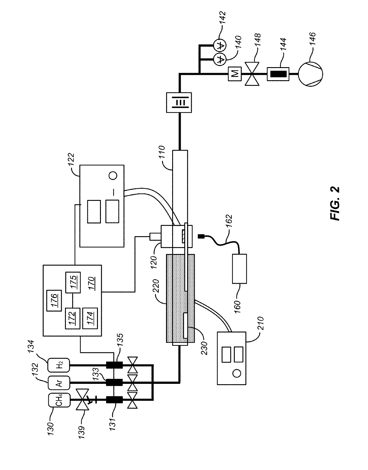
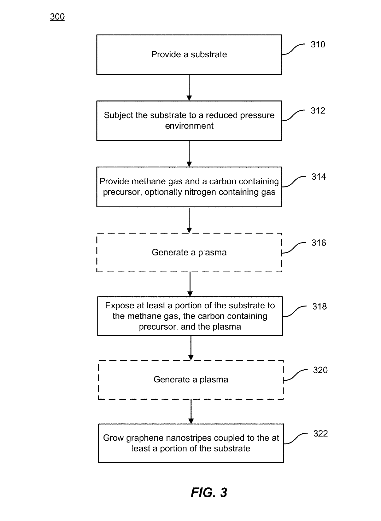
[0037]The present invention relates generally to methods and systems for material synthesis. More specifically, the present invention relates to methods and systems for growing high quality graphene nanostripes using a high-yield, single-step, low-temperature catalytic growth process. The methods and techniques can be applied to a variety of graphene growth systems including CMOS compatible semiconductor growth processes.

[0038]Without limiting embodiments of the present invention, we refer to structures described herein as graphene nanostripes, to indicate their large aspect ratios and to differentiate these graphene nanostripes from graphene nanostripes that exhibit quantum confinement and from graphene nanosheets or nanowalls that are generally wider than the graphene nanostripes discussed herein.

[0039]FIG. 1 is a simplified schematic diagram illustrating a PECVD system for growing graphene nanostripes according to an embodiment of the present invention. As illustrated in FIG. 1, ...


PUM

PropertyMeasurementUnit
temperaturesaaaaaaaaaa
frequencyaaaaaaaaaa
pressureaaaaaaaaaa

Abstract

A method of forming graphene nanostripes includes providing a substrate comprising at least one of copper foil or nickel foam and subjecting the substrate to a reduced pressure environment in a processing chamber. The method also includes providing methane gas and 1,2-dichlorobenzene (1,2-DCB) gas, flowing the methane gas and the 1,2-DCB into the processing chamber, and establishing a partial pressure ratio of 1,2-DCB gas to methane gas in the processing chamber. The partial pressure ratio is between 0 and 3. The method further includes generating a plasma, thereafter, exposing the at least a portion of the substrate to the methane gas, the 1,2-DCB gas, and the plasma, and growing the graphene nanostripes coupled to the at least a portion of the substrate.

Description

CROSS-REFERENCES TO RELATED APPLICATIONS[0001]This application claims priority to U.S. Provisional Patent Application No. 62 / 563,246, filed on Sep. 26, 2017, entitled “High-yield Single-step Low-temperature Catalytic Growth of Graphene Nanoribbons by Plasma Enhanced Chemical Vapor Deposition,” the disclosure of which is hereby incorporated by reference in its entirety for all purposes.STATEMENT AS TO RIGHTS TO INVENTIONS MADE UNDER FEDERALLY SPONSORED RESEARCH OR DEVELOPMENT[0002]N / ABACKGROUND OF THE INVENTION[0003]Graphene, a monolayer of carbon atoms forming a two-dimensional honeycomb lattice structure, is considered a wonder material for both scientific research and technological applications. Its unique electronic, thermal, and mechanical properties and compatibility with lithographic techniques are ideal for many nano-electronic, spintronic, and mechanical applications; it is also promising for large-area optoelectronic devices such as touch screen displays and electrodes for ...

Claims


Application Information

Patent Timeline
Patent Type & Authority Applications(United States)
IPC IPC(8): C23C16/513C23C16/26C01B7/01
CPCC23C16/513C23C16/26C01B7/01C01B32/186B82Y30/00B82Y40/00C23C16/4418C23C16/50C01B2204/06
Inventor YEH, NAI-CHANGHSU, CHEN-CHIH
Owner CALIFORNIA INST OF TECH
Why Eureka
Try Eureka