Semiconductor device
a technology of semiconductor devices and semiconductors, applied in semiconductor devices, digital storage, instruments, etc., can solve the problems of leakage current generation between the connection electrodes, interference of potential applied to the other wiring, etc., and achieve the effect of improving the retention characteristics of the memory
- Summary
- Abstract
- Description
- Claims
- Application Information
AI Technical Summary
Benefits of technology
Problems solved by technology
Method used
Image


Examples
embodiment 1
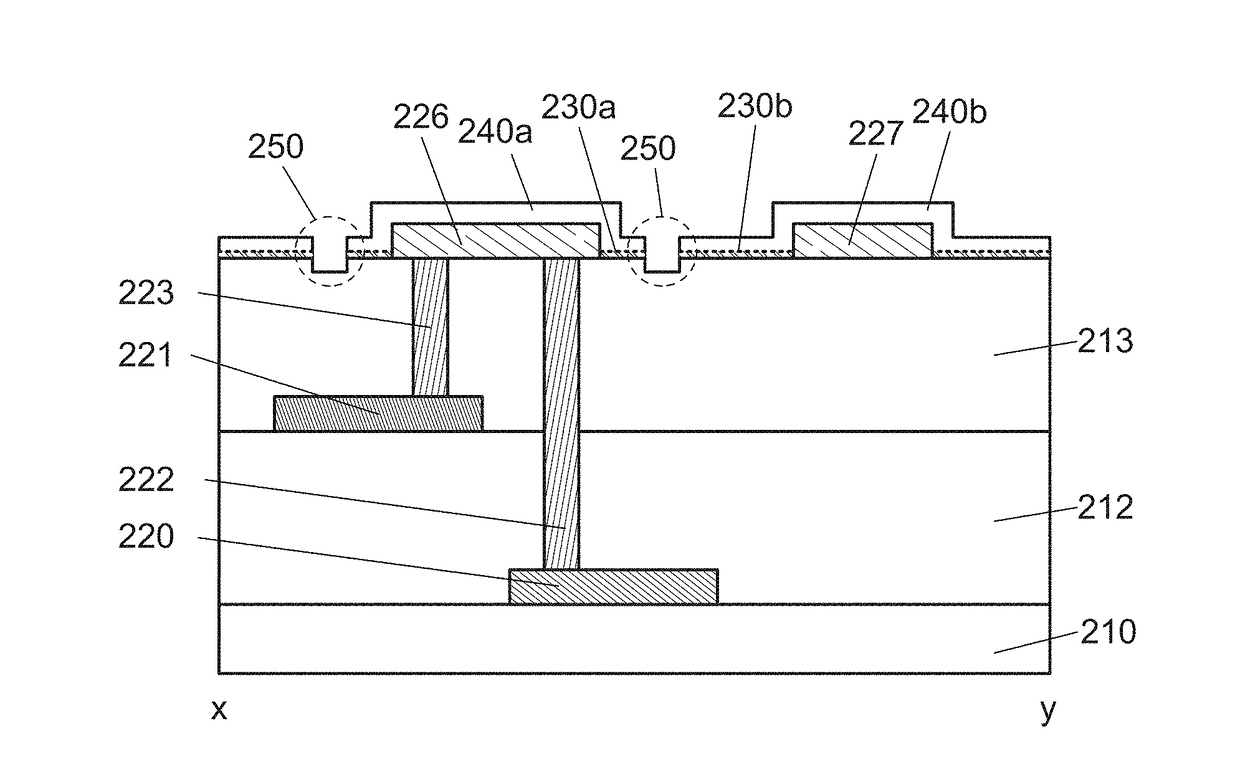
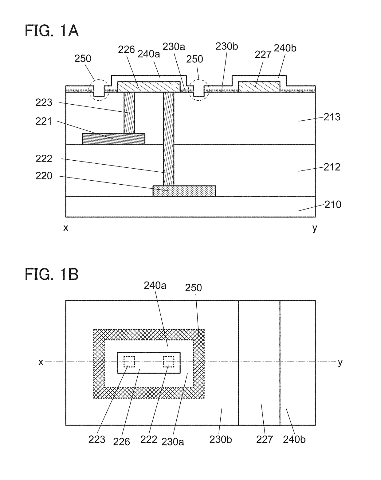
[0062]In this embodiment, structures and a manufacturing method of a semiconductor device of one embodiment of the present invention are described with reference to FIGS. 1A and 1B to FIGS. 10A to 10C. Note that in FIGS. 1A and 1B to FIGS. 10A to 10C, some components of the semiconductor device are not illustrated for clarity.
[0063]FIGS. 1A and 1B illustrate a part of a structure of a semiconductor device of one embodiment of the present invention. FIG. 1B is a schematic top view illustrating a structure of a semiconductor device. FIG. 1A corresponds to a schematic cross-sectional view taken along dashed-dotted line x-y in FIG. 1B. Note that in the top view such as FIG. 1B, a groove 250 is illustrated as a hatch pattern.
[0064]In the cross-sectional view such as FIG. 1A, end portions of some of patterned conductors, semiconductors, and insulators have right-angled corners; however, the semiconductor device in this embodiment is not limited thereto and can have rounded end portions.
[0...
embodiment 2
[0234]In this embodiment, examples of a semiconductor device (memory device) of one embodiment of the present invention are described.
[0235]FIGS. 11A to 11C show circuit examples of the semiconductor device (memory device) of one embodiment of the present invention.
[0236]The semiconductor device illustrated in FIG. 11A includes a transistor 280 using a first semiconductor material, a transistor 400 using a second semiconductor material, and a capacitor 80.
[0237]The first and second semiconductor materials preferably have different energy gaps. For example, the first semiconductor material can be a semiconductor material other than an oxide semiconductor (examples of such a semiconductor material include silicon (including strained silicon), germanium, silicon germanium, silicon carbide, gallium arsenide, aluminum gallium arsenide, indium phosphide, gallium nitride, and an organic semiconductor), and the second semiconductor material can be an oxide semiconductor. A transistor using ...
embodiment 3
[0279]In this embodiment, an example of a semiconductor device of one embodiment of the present invention is described.
[0280]Next, a transistor 400d illustrated in FIGS. 14A to 14C is described. FIGS. 14A to 14C are a top view and cross-sectional views of the transistor 400d. FIG. 14A is a top view of the transistor 400d. FIG. 14B is a cross-sectional view taken along dashed-dotted line A1-A2 in FIG. 14A. FIG. 14C is a cross-sectional view taken along dashed-dotted line A3-A4 in FIG. 14A. Note that for simplification of the drawing, some components are not illustrated in the top view of FIG. 14A.
[0281]The transistor 400d can be fabricated in parallel with the above transistor 400a or the like. In the case where the transistor 400d is fabricated in parallel with the transistor 400a, the transistor 400d can be fabricated without an extra step.
[0282]The transistor 400d is different from the transistor 400a in including an oxide 406a1 and an oxide 406a2 that are separate from each other...
PUM
 Abstract
Description
Claims
Application Information
 - R&D
- Intellectual Property
- Life Sciences
- Materials
- Tech Scout
- Unparalleled Data Quality
- Higher Quality Content
- 60% Fewer Hallucinations
Browse by: Latest US Patents, China's latest patents, Technical Efficacy Thesaurus, Application Domain, Technology Topic, Popular Technical Reports.
© 2025 PatSnap. All rights reserved.Legal|Privacy policy|Modern Slavery Act Transparency Statement|Sitemap|About US| Contact US: help@patsnap.com