Manufacturing method of amoled pixel driver circuit

a manufacturing method and driver technology, applied in the field of display techniques, can solve the problems of delay of alternating signals, large parasitic capacitance of tft, affecting the response speed of the circuit, etc., and achieve the effects of reducing the rc effect, excellent device characteristics, and small parasitic capacitan

Inactive Publication Date: 2018-08-02
SHENZHEN CHINA STAR OPTOELECTRONICS TECH CO LTD
View PDF40 Cites 0 Cited by
  • Summary
  • Abstract
  • Description
  • Claims
  • Application Information

AI Technical Summary

Benefits of technology

The present invention provides an AMOLED pixel driver circuit that can make both ES-type TFT (driving TFT) and BCE-type TFT (switching TFT) simultaneously, reduces the RC effect and helps control the alternating data signal. The BCE-type TFT has a smaller parasitic capacitance, while the ES-type TFT has better device characteristics and can provide a stable OLED current. This results in OLED light-emission stability and uniformity. The manufacturing method is simple, and only requires one insulation layer as an etch-stopping layer.

Problems solved by technology

However, ES-structure leads to large parasitic capacitance of TFT.
When used as switching TFT, large resistance-capacitance (RC) resulting in delay of alternating signals and affecting the response speed of the circuit.
However, the BCE process causes other problems, and results in poor TFT characteristics.
In the AMOLED pixel drive circuit, the use of ES-type TFT will produce a larger parasitic capacitance and increase the RC effect of data signal; on the other hand, although the use of BCE-type TFT can effectively reduce the parasitic capacitance, the TFTs from the BCE process perform less well than the ES-type TFTs, which will have a negative impact on the light-emission of OLED.

Method used


Image

  • Manufacturing method of amoled pixel driver circuit
  • Manufacturing method of amoled pixel driver circuit
  • Manufacturing method of amoled pixel driver circuit

Examples


Embodiment Construction

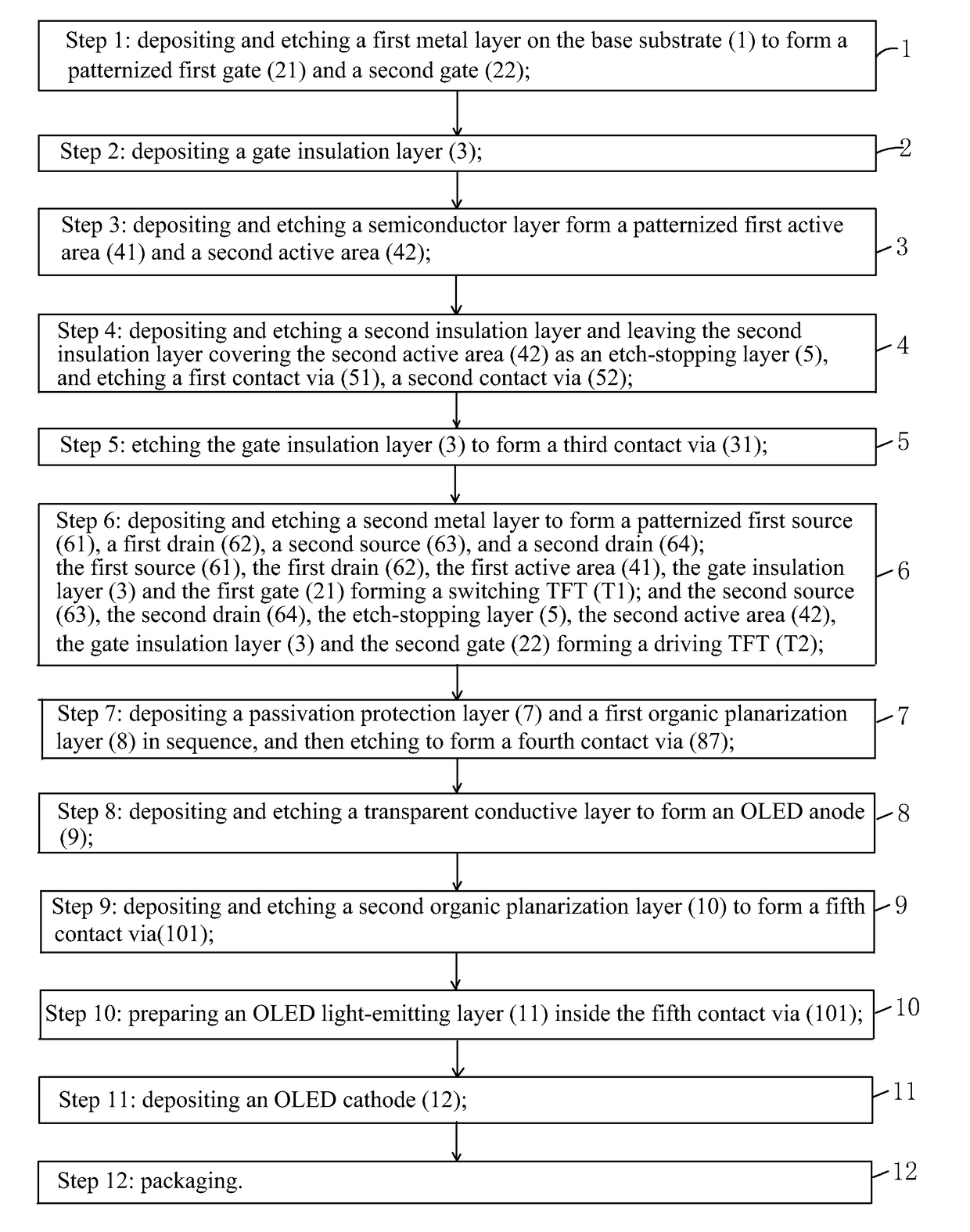
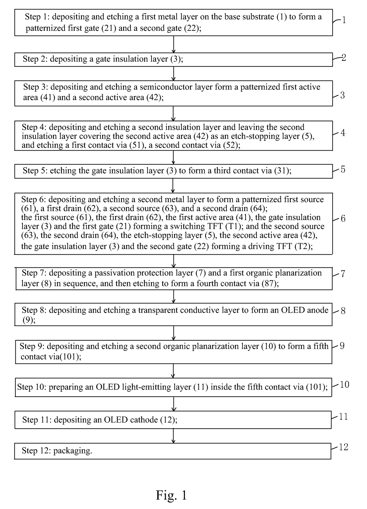
[0061]Referring to FIG. 1, the present invention provides a manufacturing method of AMOLED pixel driver circuit, which comprises the following steps:

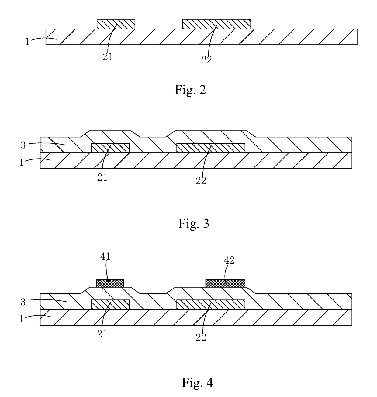
[0062]Step 1: as shown in FIG. 2, providing a base substrate 1, depositing and etching a first metal layer on the base substrate 1 to form a patternized first gate 21 and a second gate 22.

[0063]Specifically, the substrate is a transparent substrate, and preferably, a glass substrate.

[0064]The material of the first metal layer is a stack combination of one or more of molybdenum (Mo), titanium (Ti), aluminum (Al), copper (Cu) and silver (Ag).

[0065]Step 2: as shown in FIG. 3, depositing a gate insulation layer 3 to cover the base substrate 1, the first gate 21 and the second gate 22.

[0066]Specifically, the material for the gate insulation layer is silicon oxide (SiOx), silicon nitride (SiNx), or a combination of the two.

[0067]Step 3: as shown in FIG. 4, depositing and etching a semiconductor layer on the gate insulation layer 3 to form a p...


PUM


Abstract

The invention provides a manufacturing method of AMOLED pixel driver circuit, by leaving only a second insulation layer (5) covering the second active area (42) as an etch-stopping layer, making an ES-type driving TFT (T2), and a BCE-type switching TFT (T1). BCE-type switching TFT (T1) has a smaller parasitic capacitance, can reduce the RC effect, and is good for controlling the alternating data signal; ES-type driving TFT (T2) has excellent device characteristics, and can provide a stable OLED current to ensure the stability and uniformity of OLED light-emission.

Description

BACKGROUND OF THE INVENTION1. Field of the Invention[0001]The present invention relates to the field of display techniques, and in particular to a manufacturing method of AMOLED pixel driver and thereof.2. The Related Arts[0002]The organic light emitting diode (OLED) display provides the advantages of active light-emitting, low driving voltage, high emission efficiency, quick response time, high resolution and contrast, near 180° viewing angle, wide operation temperature range, and capability to realize flexible display and large-area full-color display, and is regarded as the most promising display technology.[0003]The driving types of OLED can be divided, according to the driving method, into the passive matrix OLED (PMOLED) and active matrix OLED (AMOLED), i.e., the direct addressable type and thin film transistor (TFT) addressable type, wherein the AMOLED provides the advantages of pixels arranged in an array, self-luminous, and high luminous efficiency and is commonly used for ...

Claims


Application Information

Patent Timeline
IPC IPC(8): H01L51/56H01L27/32H01L51/52H01L51/00
CPCH01L51/56H01L27/3262H01L51/5221H01L51/5206H01L51/0005H01L2227/323H10K59/1213H10K59/12H10K71/00H10K71/135H01L27/1248H01L27/1251H10K59/1201H01L29/66765H01L27/1225H01L27/1214H01L27/1222H01L27/1218H01L27/127H10K10/88H10K10/466H10K10/472H10K10/474H10K50/81H10K50/82H10K50/822H10K59/123H10K59/124H10K59/125H10K71/231H10K71/621H10K10/84H10K10/484
Inventor CHI, SHIPENGWU, YUANCHUN
Owner SHENZHEN CHINA STAR OPTOELECTRONICS TECH CO LTD
Why Eureka
Try Eureka