Forming method of semiconductor component

A semiconductor and device technology, applied in the field of semiconductor device formation, can solve the problems of large RC effect and poor performance of semiconductor integrated circuits, and achieve the effects of improving performance, reducing RC effect, and avoiding collapse

Active Publication Date: 2015-04-01
SEMICON MFG INT (SHANGHAI) CORP
View PDF5 Cites 0 Cited by
  • Summary
  • Abstract
  • Description
  • Claims
  • Application Information

AI Technical Summary

Problems solved by technology

[0010] However, the RC effect of semiconductor devices formed by existing technologies is still large, and the performance of semiconductor integrated circuits is poor

Method used


Image

  • Forming method of semiconductor component
  • Forming method of semiconductor component
  • Forming method of semiconductor component

Examples


Embodiment Construction

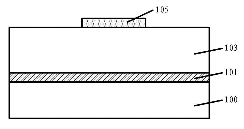
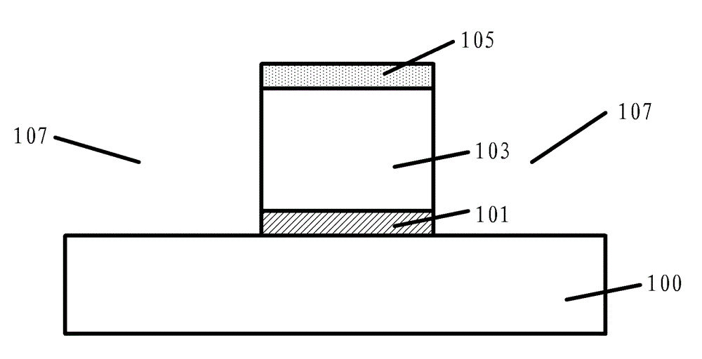
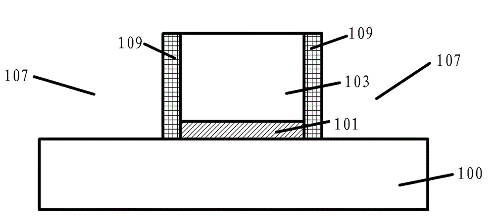
[0042] As mentioned in the background, the RC effect of the semiconductor device in the prior art is still relatively large, and the performance of the semiconductor integrated circuit is poor.

[0043] After research, the inventors found that in the prior art, when the opening is formed, if the size (width) of the opening is too large, the material used to form the insulating layer will fall into the opening when the insulating layer is subsequently formed, making it difficult to deposit the insulating layer. , it is difficult to form an insulating layer covering the metal line and across the opening, and even if the insulating layer is formed, the quality of the void gap is greatly affected. Therefore, limited by the subsequent deposition process, the size (width) of the air gap formed in the prior art is usually small, and the K value in the interconnection structure that can be reduced by the small air gap is relatively limited. The semiconductor device The RC effect is st...


PUM

PropertyMeasurementUnit
sizeaaaaaaaaaa

Abstract

A forming method of a semiconductor component comprises the steps of providing a substrate, wherein a first sacrificial layer, an interlayer dielectric layer and at least two grooves are sequentially formed in the surface of the substrate, and the grooves penetrate through the interlayer dielectric layer and the first sacrificial layer, processing the portions, on the side walls of the grooves, of the interlayer dielectric layer, forming a second sacrificial layer, filling conductive materials inside the grooves after formation of the second sacrificial layer, forming a metal wire layer, forming a first mask layer, wherein the first mask layer is covered on the metal wire layer and a part of the second sacrificial layer so as to enable the rest part of the second sacrificial layer and the first sacrificial layer not to be eliminated, eliminating the portion, exposed out of the first mask layer, of the second sacrificial layer and the portion, at the bottom of the second sacrificial layer, of the first sacrificial layer, forming an opening, eliminating a second mask layer, and forming an insulating layer which is covered on the metal wire layer, the rest of the second sacrificial layer and the interlayer dielectric layer, and stretches across the opening. A semiconductor integrated circuit formed by the method of the semiconductor component is small in resistance-capacitance (RC) effect and good in performance.

Description

technical field [0001] The invention relates to the technical field of semiconductor manufacturing, in particular to a method for forming a semiconductor device. Background technique [0002] As the semiconductor industry enters a new era of high-performance and multi-functional integrated circuits, the density of components in integrated circuits will increase, while the size of components and the spacing between parts or components will decrease accordingly. In the past, it was only limited by the ability of lithographic technology to define the structure, and it was difficult to make the geometric size of the device smaller; with the development of technology, the size of existing devices can be made smaller, but new limiting factors are becoming more and more many. For example, when the distance between the conductive patterns decreases, the capacitance generated by any two adjacent conductive patterns (which is a function of the dielectric constant K of the insulating ...

Claims


Application Information

Patent Timeline
Patent Type & Authority Patents(China)
IPC IPC(8): H01L21/768
Inventor 洪中山
Owner SEMICON MFG INT (SHANGHAI) CORP
Why Eureka
Try Eureka