Forming method of air gap in interconnection layer

A technology of air gap and interconnection layer, applied in the direction of electrical components, semiconductor/solid-state device manufacturing, circuits, etc., can solve the problems of poor performance of semiconductor integrated circuits, achieve the effect of reducing RC effect, improving performance, and uniform width

Active Publication Date: 2015-04-29
SEMICON MFG INT (SHANGHAI) CORP
View PDF4 Cites 0 Cited by
  • Summary
  • Abstract
  • Description
  • Claims
  • Application Information

AI Technical Summary

Problems solved by technology

[0009] However, the performance of semiconductor integrated circuits after the formation of air gaps in the interconnection layer using the prior art is poor

Method used


Image

  • Forming method of air gap in interconnection layer
  • Forming method of air gap in interconnection layer
  • Forming method of air gap in interconnection layer

Examples


Embodiment Construction

[0042] As mentioned in the background, the prior art semiconductor integrated circuit has poor performance after air gaps are formed in the interconnection layer.

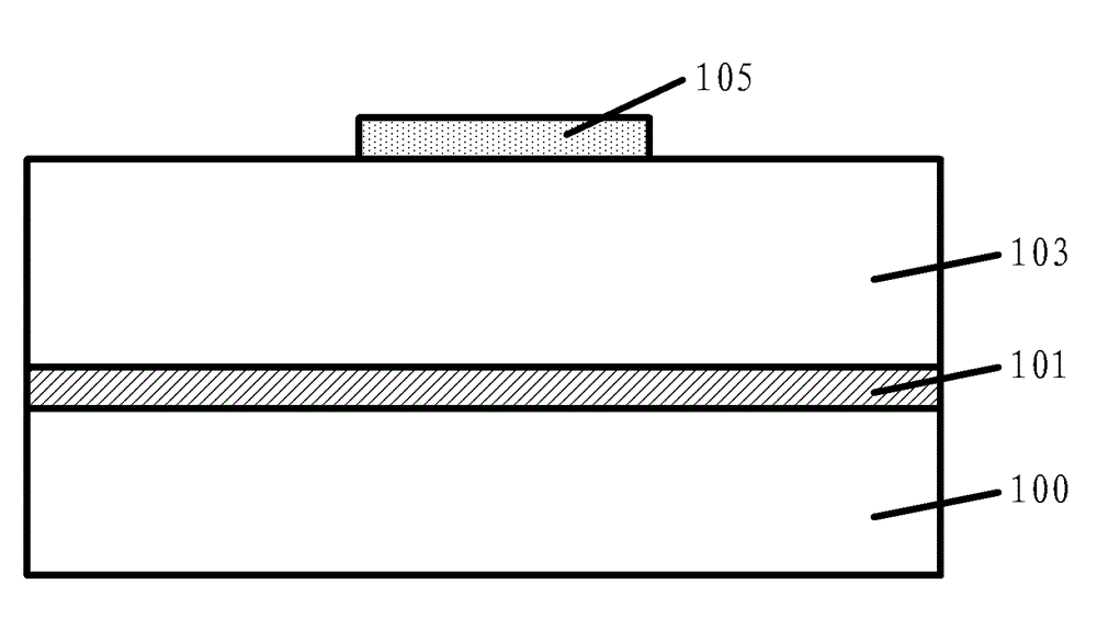
[0043] After doing your research, go ahead and refer to Figure 5 The inventors found that the reason for the poor performance of the semiconductor integrated circuit in the prior art is that there are more interlayer dielectric layers 103 between two adjacent trenches, resulting in a higher effective K value in the interconnection layer.

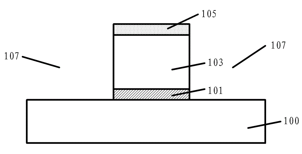
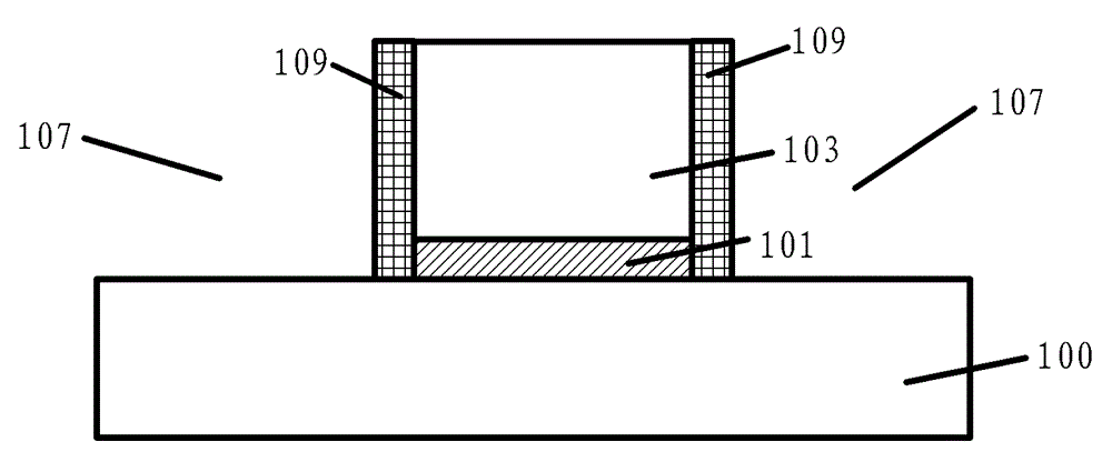
[0044] The inventors have found that if a sacrificial layer is formed by oxidizing the sidewall of the trench 107 without using a deposition process, the process steps can be reduced. Please refer to figure 2 , removing the patterned photoresist layer 105 by using an ashing process (please refer to figure 2 ) while oxidizing the interlayer dielectric layer 103 on the sidewall of the trench 107 to form a sacrificial layer, and then filling the trench 107 with conductive metal ...


PUM


Abstract

An embodiment of the invention provides a forming method of an air gap in an interconnection layer. The forming method of the air gap in the interconnection layer comprises that a semiconductor substrate is provided, and an inter-lamination dielectric layer, a hard mask layer and a photoresist layer with an opening are sequentially formed on the surface of the semiconductor substrate; the photoresist layer is used as a mask for etching the hard mask layer to transfer the opening to the inside of the hard mask layer; after the hard mask layer is etched, the photoresist layer is removed; after the photoresist layer is removed, the hard mask layer with the opening is used as a mask for etching the inter-lamination dielectric layer to form a groove, wherein the surface of the semiconductor substrate is exposed to the surface the groove; a sacrificial layer is formed and is arranged on the lateral wall of the groove; the groove is filled up to form electric leads, and the sacrificial layer is removed to form the air gas. A semiconductor integrated circuit of the forming method of the air gap in the interconnection layer is good in performance.

Description

technical field [0001] The invention relates to the technical field of semiconductor manufacturing, in particular to a method for forming an air gap in an interconnection layer. Background technique [0002] As the semiconductor industry enters a new era of high-performance and multi-functional integrated circuits, the density of components in integrated circuits will increase, while the size of components and the spacing between parts or components will decrease accordingly. In the past, the achievement of the above objectives was limited only by the ability of photolithography to define the structure. In the prior art, the geometric features of the components with smaller dimensions have created new limiting factors. For example, when the distance between the conductive patterns decreases, the capacitance generated by any two adjacent conductive patterns (which is a function of the dielectric constant K of the insulating material used to separate the distance between the c...

Claims


Application Information

Patent Timeline
Patent Type & Authority Patents(China)
IPC IPC(8): H01L21/768
Inventor 洪中山
Owner SEMICON MFG INT (SHANGHAI) CORP
Why Eureka
Try Eureka