Process for Forming a Cobalt-Iron Alloy Film on a Substrate
- Summary
- Abstract
- Description
- Claims
- Application Information
AI Technical Summary
Benefits of technology
Problems solved by technology
Method used
Image
Examples
first embodiment
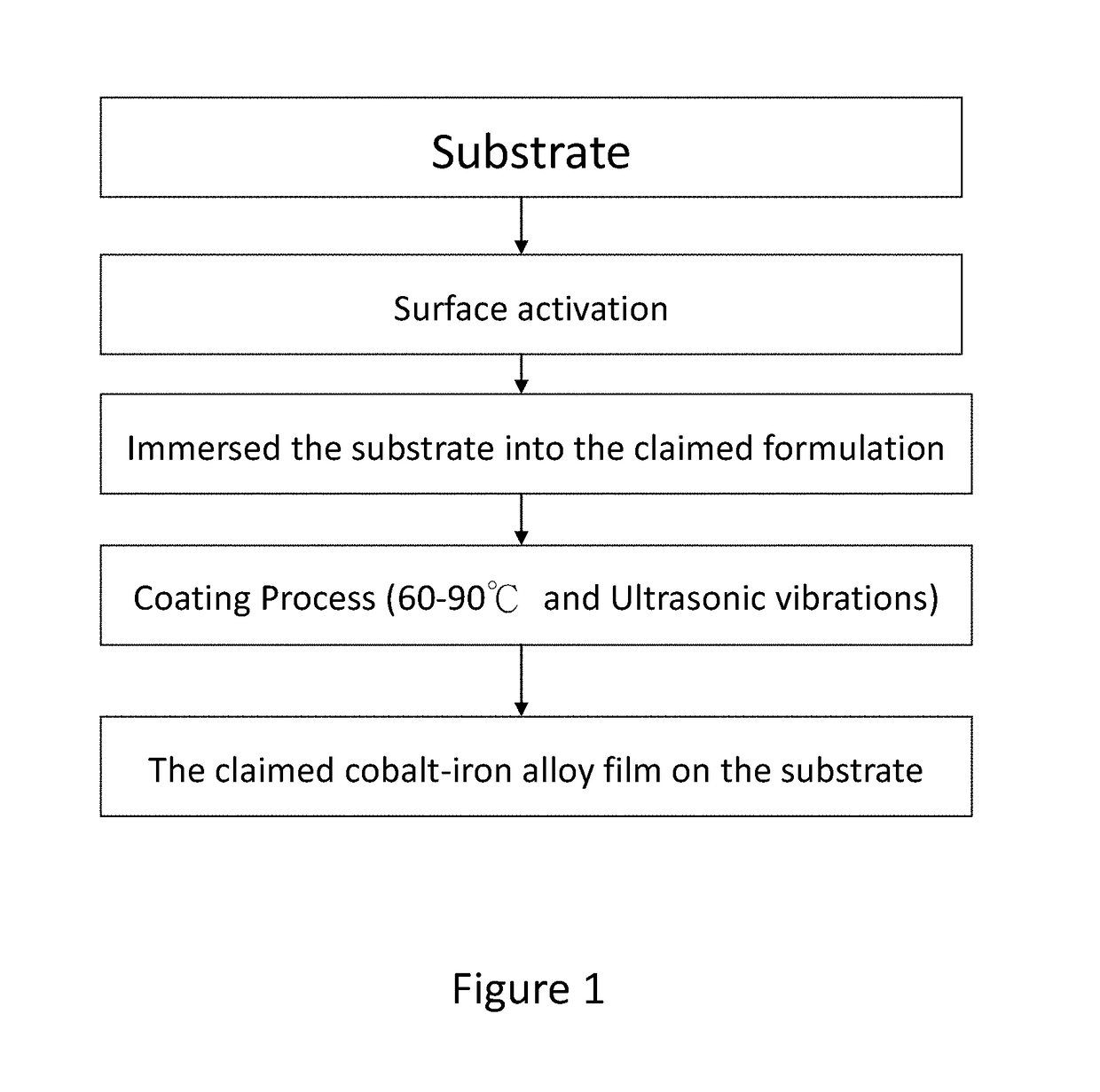
[0033]In the present invention, a process for forming a cobalt-iron alloy film on a substrate is disclosed. The process as shown in FIG. 1 comprises the following steps provide a substrate; apply surface activation treatment to surfaces of the substrate to produce activated surfaces; provide a formulation which comprises a cobalt compound, a iron compound and a phosphorus compound and perform a coating process operated at 60-90° C. and under ultrasonic vibrations simultaneously to have the formulation form a cobalt-iron alloy film on the activated surfaces. The content of the cobalt-iron alloy film comprises about 75-95wt. % of cobalt, 4.5-20 wt. % of iron and 0.5-5 wt. % of phosphorus.
[0034]In one example of the first embodiment, the substrate is made of one selected from the group consisting of Cu, Au, Al, Si, C and Al2O3. Preferably, the substrate is Cu.
[0035]In one example of the first embodiment, the surface activation treatment is performed in the presence of a palladium compo...
second embodiment
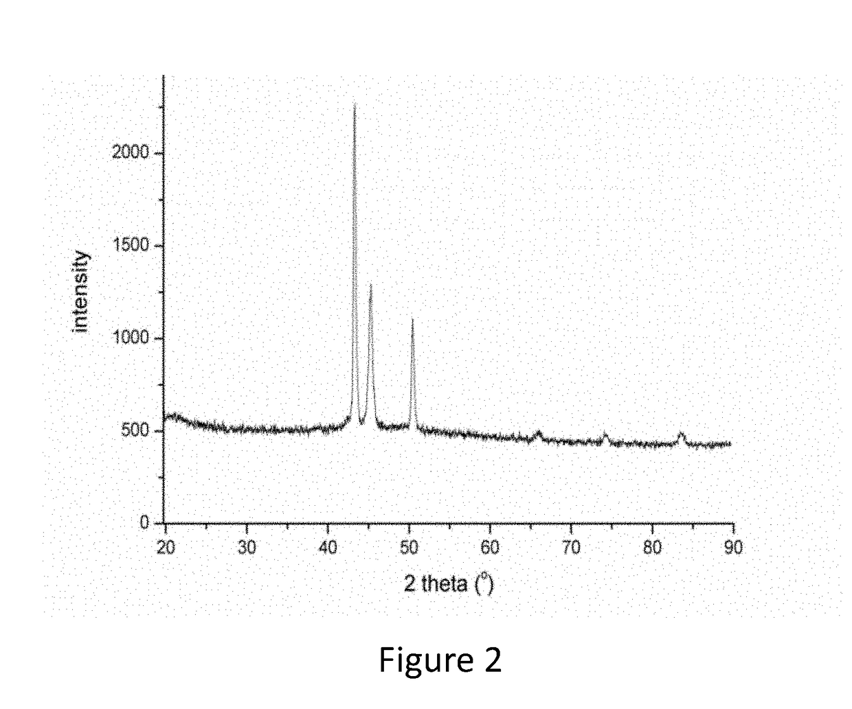
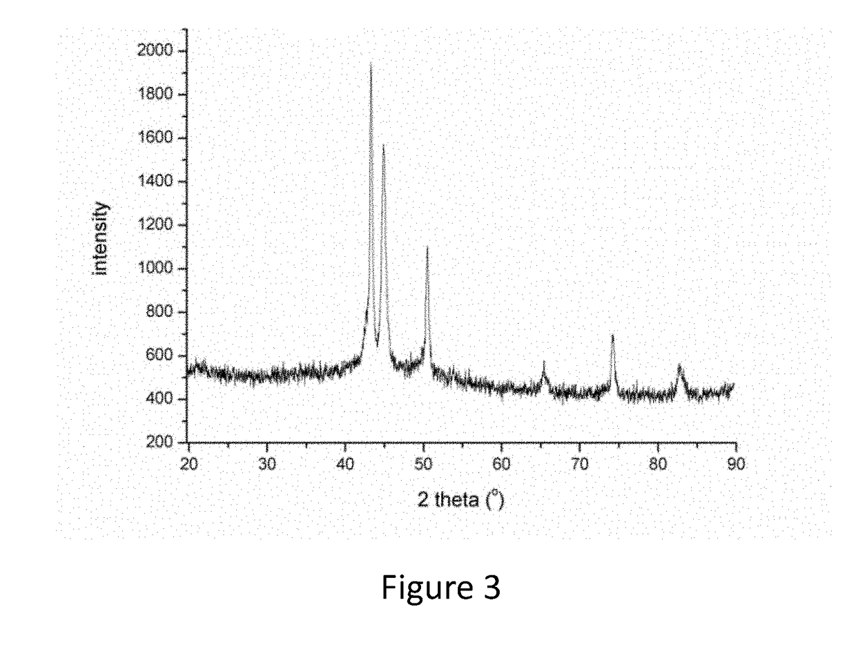
[0049]In a second embodiment, a cobalt-iron alloy film which consists of about 75-95wt. % of cobalt, 4.5-20 wt. % of iron and 0.5-5 wt. % of phosphorus is disclosed. In addition, the claimed cobalt-iron alloy film also comprises peaks at about 43.2±0.2, 45.1±0.2, 50.4±0.2, 65.5+0.2, 74.1±0.2 and 83.2±0.2 2-theta degree in X-ray powder diffraction pattern.
[0050]In a certain example of the second embodiment, the X-ray powder diffraction pattern of the cobalt-iron alloy film is shown in FIG. 3.
[0051]In another example of the second embodiment, the cobalt-iron alloy film has a thickness between 200 nm and 2000 nm.
[0052]In another example of the second embodiment, the cobalt-iron alloy film is part of a flip chip packaging, chip scale packaging or wafer level chip scale packaging.
[0053]In another example of the second embodiment, the cobalt-iron alloy film is part of a printed circuit board or a light-emitting diode device.
[0054]Accordingly, the present invention discloses a process for ...
PUM
| Property | Measurement | Unit |
|---|---|---|
| Temperature | aaaaa | aaaaa |
| Thickness | aaaaa | aaaaa |
| Thickness | aaaaa | aaaaa |
Abstract
Description
Claims
Application Information
 - R&D
- Intellectual Property
- Life Sciences
- Materials
- Tech Scout
- Unparalleled Data Quality
- Higher Quality Content
- 60% Fewer Hallucinations
Browse by: Latest US Patents, China's latest patents, Technical Efficacy Thesaurus, Application Domain, Technology Topic, Popular Technical Reports.
© 2025 PatSnap. All rights reserved.Legal|Privacy policy|Modern Slavery Act Transparency Statement|Sitemap|About US| Contact US: help@patsnap.com


