Selectively activated synaptic device with ultrasmall dimension and low power consumption

a synaptic device and ultra-small dimension technology, applied in the field of capacitors, can solve the problems of limited programming time, greater total thickness of conductive bridge memory-based synaptic devices, and inability to transfer between stp and ltp by stimulation

Active Publication Date: 2018-01-18
KONKUK UNIV IND COOP CORP
View PDF0 Cites 8 Cited by
  • Summary
  • Abstract
  • Description
  • Claims
  • Application Information

AI Technical Summary

Benefits of technology

[0007]The present disclosure provides a high-performance capacitor capable of selectively regulating synaptic plasticity by controlling the migration of active electrode ions through simultaneous use of an external electric field and an internal electric field due to polarization of the inside of a ferroelectric thin film, a memory device including the same, and a method of manufacturing the capacitor.

Problems solved by technology

However, the transition between STP and LTP by stimulation has not been reported in FTJ-based synaptic devices.
However, a total thickness of conductive bridge memory-based synaptic devices is greater than that of a single FTJ-based synaptic device, and shortening of its programming time is limited by the migration of cations through nanogaps.
In addition, in FTJ-based or conductive bridge memory-based synaptic devices, selective synaptic plasticity without the aid of external selection devices has not been reported.
However, a neuromorphic device using cation migration has a limitation in implementation of low power and high integration, and a neuromorphic device using ferroelectric polarization inversion has a low on / off ratio problem and a difficulty in simultaneously realizing volatility and non-volatility.
In addition, neuromorphic devices themselves do not have selectivity functions and thus additional selection devices are needed.

Method used


Image

  • Selectively activated synaptic device with ultrasmall dimension and low power consumption
  • Selectively activated synaptic device with ultrasmall dimension and low power consumption
  • Selectively activated synaptic device with ultrasmall dimension and low power consumption

Examples


example 1

Manufacture of Ferroelectric Tunnel Junction (FTJ) Device

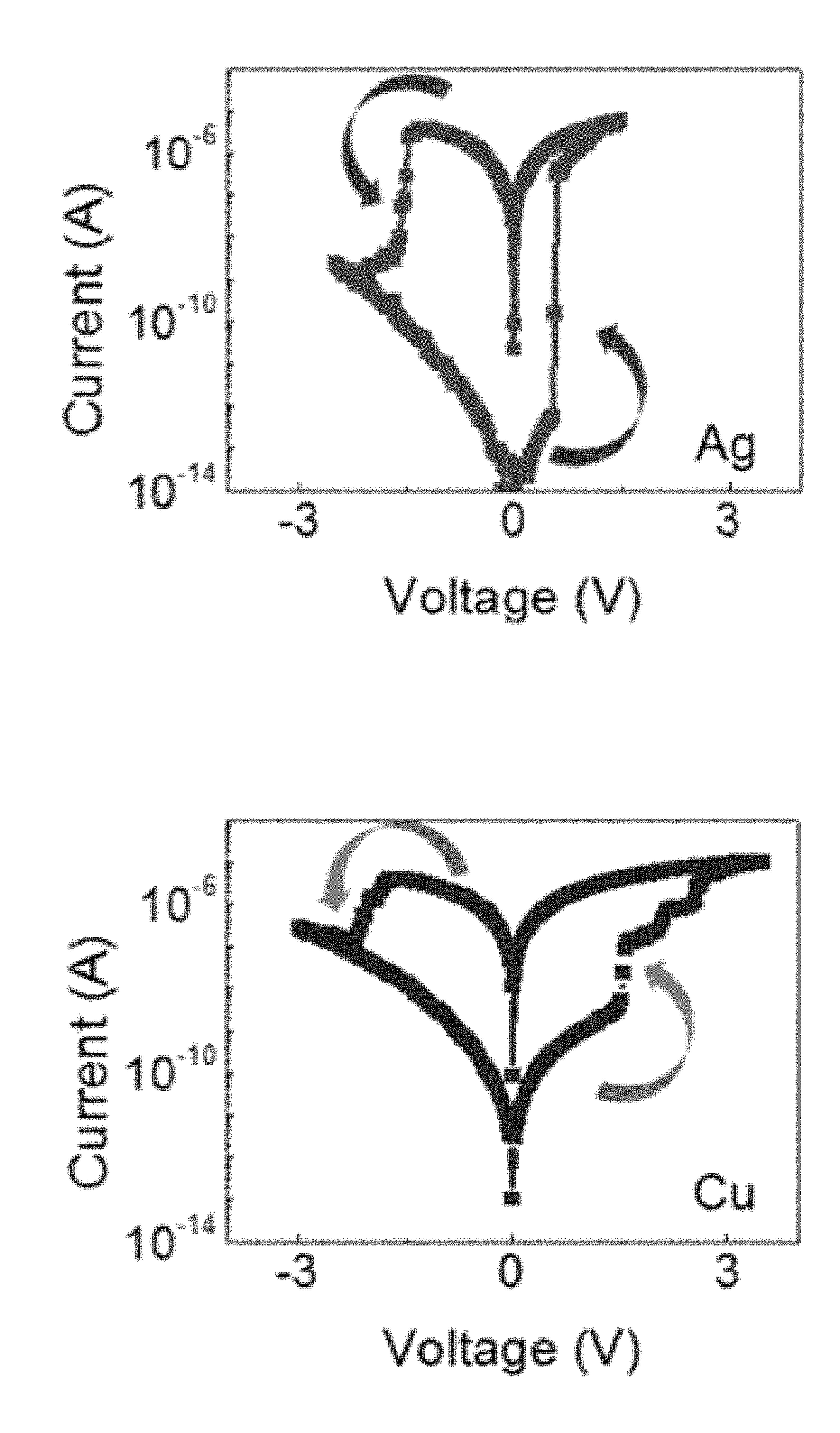
[0068]A thin film having a PZT / LSMO heterostructure was grown on a monocrystalline SrTiO3 (001) substrate by PLD using a KrF excimer laser (λ=248 nm). An energy density of the laser beam (1 Hz repetition rate) irradiated on the rotating LSMO and PZT targets was 1 J / cm2. The LSMO and PZT films were deposited at an oxygen pressure of 100 mTorr and 200 mTorr, respectively and 675° C. and 550° C., respectively. After deposition, the PZT / LSMO films were heat-treated at 550° C. for 30 minutes at an oxygen pressure of 300 mTorr, and then cooled at a rate of 5° C. / min. To manufacture an FTJ device, Ag (40 nm) upper electrodes having sizes of 0.6×0.6 μm2 and 1.1×1.1 μm2 were formed on the PZT / LSMO heterostructure by e-beam lithography and e-beam evaporation, followed by a liftoff process.

example 2

[0069]An FTJ device was manufactured in the same manner as in Example 1, except that Cu (40 nm) upper electrodes having sizes of 0.6×0.6 μm2 and 1.1×1.1 μm2 were formed on the PZT / LSMO heterostructure by e-beam lithography and e-beam evaporation.

experimental example

Structural Characteristics

[0073]High resolution-transmission electron microscopy (HR-TEM) images were acquired using a 300 kV field emission-TEM (Tecnai G2 F30 super-twin). The thicknesses of thin films were measured using HR-TEM images.

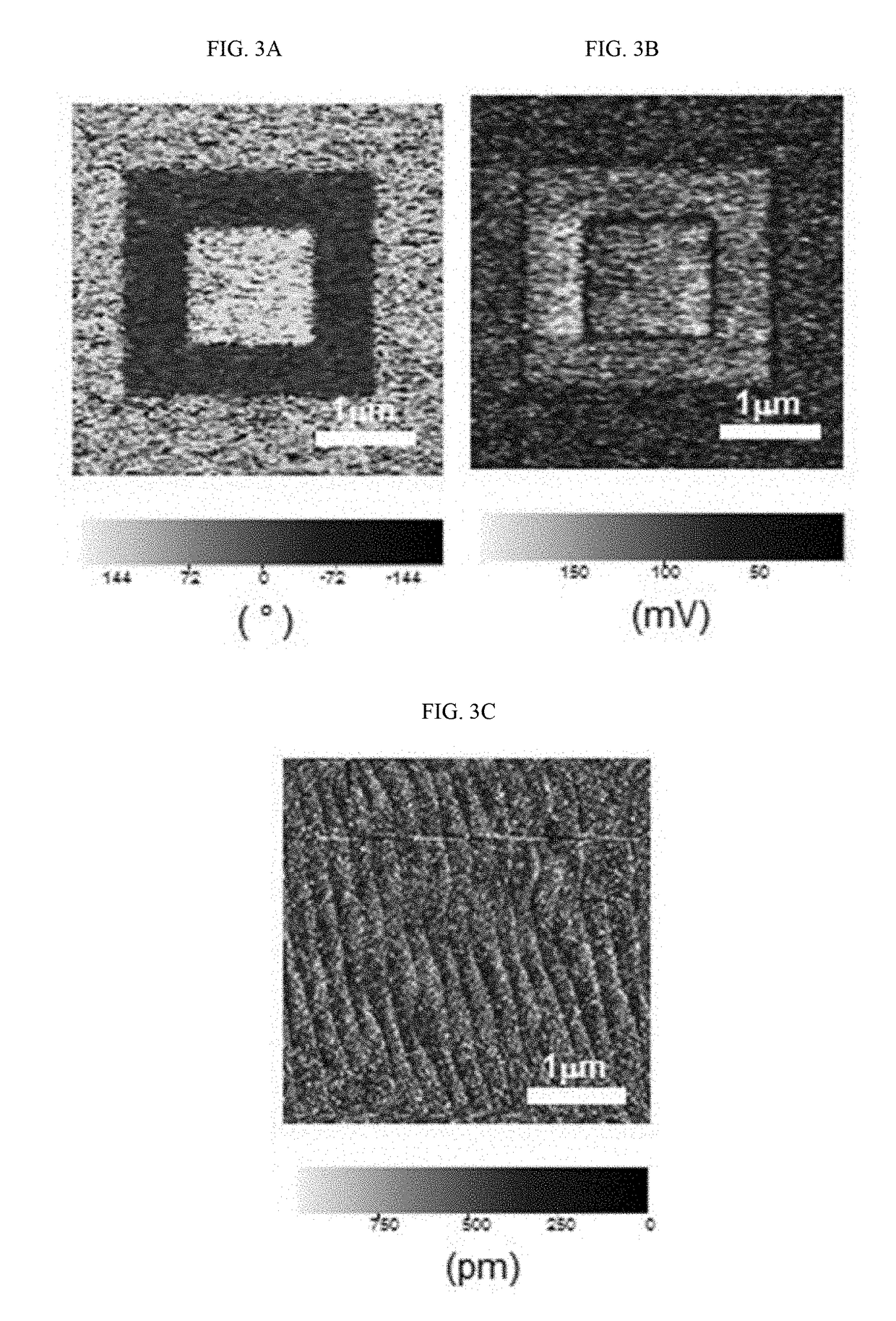
Piezoresponse Force Microscopy (PFM)

[0074]PFM images and local magnetic hysteresis curves were measured using a Pt / Ir coated cantilever and an atomic force microscope (AFM, Park Systems, XE-100). A lock-in amplifier (Stanford Research Systems, SR830) was used after applying an AC voltage (ƒ=15 kHZ) having a peak to peak amplitude of 1.0 V in a PFM mode.

Electrical Measurement

[0075]I-V characteristics were measured using a semiconductor parameter analyzer (Agilent, 4156B) and an AFM (Seiko, SPA-300 HV) in a DC voltage sweep mode. A pulse mode was used to provide pulse stimulation during gradual current modulation using a semiconductor characterization system (Keithley, 4200-SCS) and an AFM. All electrical measurements were performed in air at room temp...


PUM


Abstract

Provided herein are a capacitor, a memory device including the capacitor, and a method of manufacturing the capacitor. The capacitor is manufactured by directly depositing a metal electrode having high ion mobility on an ultrathin ferroelectric layer having a certain thickness, and thus may simultaneously use metal cation migration and ferroelectric polarization inversion, and a low-power and high-performance capacitor capable of being selectively activated may be provided by simultaneously controlling an external electric field and an internal electric field caused by polarization of the inside of a ferroelectric thin film.

Description

CROSS-REFERENCE TO RELATED APPLICATIONS[0001]This application claims priority under 35 USC §119(a) of Korean Patent Application No. 10-2016-0083260 filed on Jul. 1, 2016, the subject matter of which is hereby incorporated by reference.BACKGROUND OF THE INVENTION1. Field of the Invention[0002]The present disclosure relates to a capacitor, a memory device including the same, and a method of manufacturing the capacitor.2. Discussion of Related Art[0003]In neuromorphic computing, synapses play a key role by changing their connection strength between two neurons, as is known as synaptic plasticity. The synaptic plasticity on which the brain's memorizing ability is based may be classified as short-term plasticity (STP) and long-term potentiation (LTP) that are respectively achieved through temporal reinforcement and permanent reinforcement of synaptic connections. Memristors with gradually changing conductivity are also applicable to mimic neuromorphic computing performed by biological sy...

Claims


Application Information

Patent Timeline
Patent Type & Authority Applications(United States)
IPC IPC(8): G11C11/22H01L49/02
CPCG11C11/221H01L27/11502H01L28/55H01L28/60H10N70/245H10N70/841H10N70/8836H10N70/026H10N70/826H10B53/30H01L21/0274H01L27/0805H01L28/56H01L28/75H01L29/516H10B53/00
Inventor PARK, BAE HOYOON, CHANSOO
Owner KONKUK UNIV IND COOP CORP
Why Eureka
Try Eureka