
Method of producing dielectric material

a dielectric material and dielectric technology, applied in the direction of fixed capacitors, thin/thick film capacitors, silicon organic compounds, etc., can solve the problems of deterioration of the dispersed dielectric material grains of a product, difficult to keep the cost of production low, and large grains becoming more likely to be generated, so as to achieve high reliability, low scattering of withstand voltage properties, and high dispersion

Pending Publication Date: 2018-01-11
MURATA MFG CO LTD
View PDF7 Cites 0 Cited by
  • Summary
  • Abstract
  • Description
  • Claims
  • Application Information

AI Technical Summary

Benefits of technology

The present invention provides a method to produce a dielectric material using an aqueous slurry that has uniform distribution of metal elements and a Si component on the surface of dielectric powder with reduced risk of heat generation and suppression of inter-grain sintering. This results in a high reliability and low scattering of withstand voltage property in multilayer ceramic capacitors.

Problems solved by technology

In the technique disclosed in Patent Document 1, since an organic solvent is used, an explosion-proof apparatus or an explosion-proof facility is needed for production of a dielectric material, and thus it is difficult to keep the cost for production low.
If the organic matter is added, problems such as a problem in a molded body caused by a reaction with a binder for molding and occurrence of a crack in a sintered body caused by decomposition of the organic matter arise when molding and firing the powder including the organic matter, and thus a heat treatment process for decomposing and removing the organic matter in the dielectric material powder is typically provided before performing the molding.
There is a problem that, for example, sintering is promoted by heat generated by the decomposition of the organic matter during this heat treatment, and thus large grains become more likely to be generated and dispersion of dielectric material grains of a product deteriorates.
Therefore, there is a problem that agglomeration of silicon compound occurs at the time of addition of various metal salts and thus it is difficult to form microscopically uniform coating.

Method used


Image

  • Method of producing dielectric material
  • Method of producing dielectric material
  • Method of producing dielectric material

Examples


first exemplary embodiment (

1. First Exemplary Embodiment (Method of Producing Dielectric Material Using Alkoxysilane as Organic Silicon Compound)

[0058]In a first exemplary embodiment, a method of producing a dielectric material in the case of using an alkoxysilane as an organic silicon compound will be described.

[0059](1) Preparation Step of Preparing Slurry

[0060]First, a slurry is prepared by mixing dielectric powder, water, one of an organic-acid metal salt and an inorganic metal salt, and alkoxysilane.

[0061]Powder of a perovskite-type compound including Ba and Ti is preferable as the dielectric powder. Specific examples of the perovskite-type compound include perovskite-type compounds represented by a general formula ABO3 (A sites correspond to Ba and may include at least one selected from a group consisting of Sr and Ca in addition to Ba; B sites correspond to Ti and may include at least one selected from a group consisting of Zr and Hf in addition to Ti; and O corresponds to oxygen).

[0062]In addition, pr...

second exemplary embodiment (

2. Second Exemplary Embodiment (Method of Producing Dielectric Material Using Water-Soluble Silane Coupling Agent as Organic Silicon Compound)

[0115]Next, as a second exemplary embodiment, a method of producing a dielectric material in the case of using a water-soluble silane coupling agent as an organic silicon compound will be described. Whereas an alkoxysilane is used as the organic silicon compound in the first exemplary embodiment, in the second exemplary embodiment, contrary to the first exemplary embodiment, a water-soluble silane coupling agent is used as the organic silicon compound.

[0116](1) Preparation Step of Preparing Slurry

[0117]First, a slurry is prepared by mixing dielectric powder, water, one of an organic-acid metal salt and an inorganic metal salt, and a water-soluble silane coupling agent.

[0118]Since the dielectric powder, water, and one of organic-acid metal salt and inorganic metal salt that are used have been described in the first exemplary embodiment, the des...

example 1

[0149]In 300 g of water, 1.76 g of dysprosium acetate and 0.53 g of manganese acetate were added, mixed and stirred, and thus an aqueous solution in which dysprosium acetate and manganese acetate were dissolved in water was prepared. To this, 100 g of grains of barium titanate (hereinafter referred to as BT grains) having an average grain diameter of 150 nm were added, and thus a slurry was prepared. To the prepared slurry, 2.1 g of 3-aminopropyltrimethoxysilane was added, stirring was performed for 30 minutes, and thus a slurry was prepared.

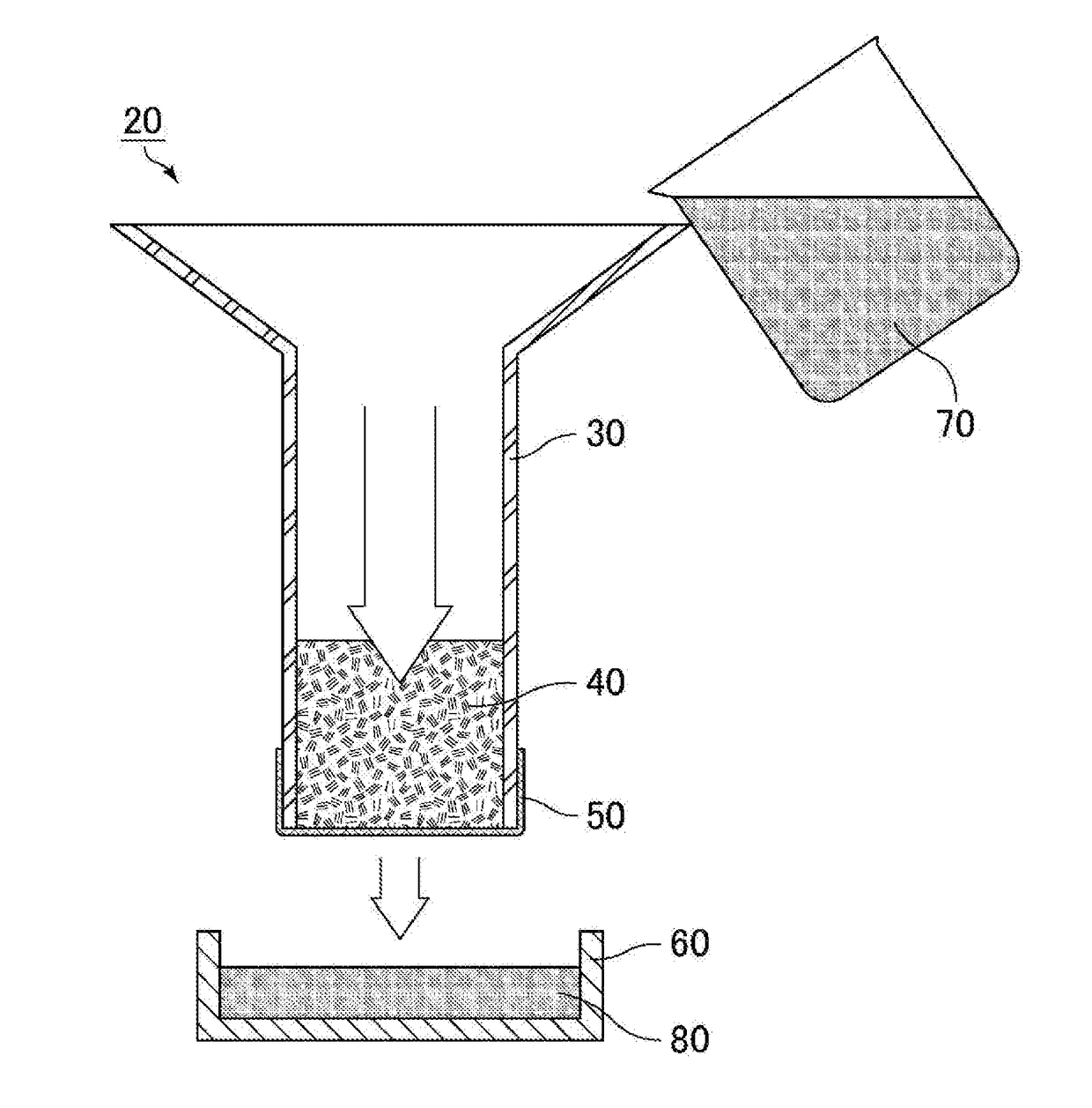
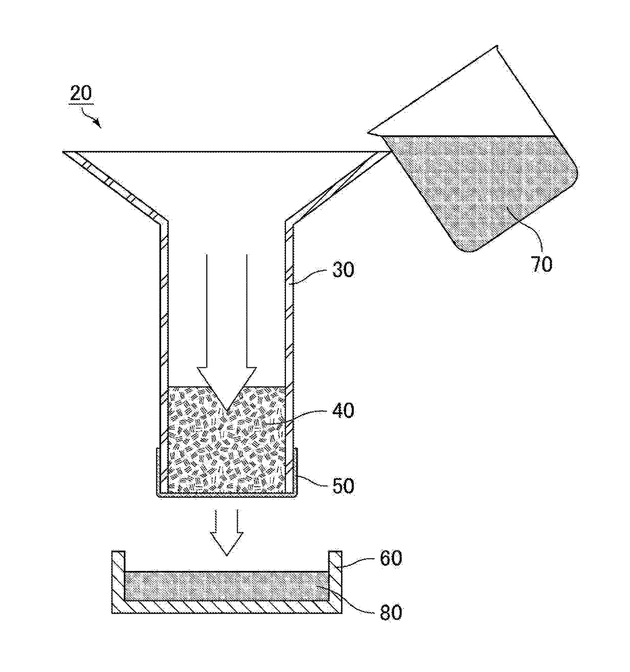
[0150]Next, an anion removing apparatus 20 as illustrated in the FIGURE was prepared.

[0151]That is, one end of a plastic cylinder 30 was covered by a mesh 50 to prevent an anion exchange resin from falling off, and then 200 ml of an anion exchange resin 40 (DIAION (registered trademark) SA10A-OH type available from Mitsubishi Chemical Corporation) was injected.

[0152]Next, a prepared slurry 70 was injected in the anion removing apparatus 20 prepa...


PUM

PropertyMeasurementUnit
temperatureaaaaaaaaaa
particle diameteraaaaaaaaaa

Abstract

A method of producing a dielectric material by preparing a slurry by mixing a dielectric powder, water, one of an organic-acid metal salt and an inorganic metal salt, and an organic silicon compound, causing the slurry to come into contact with an anion exchange resin to remove an anion derived from the one of the organic-acid metal salt and the inorganic metal salt from the slurry, and drying the slurry to obtain the dielectric material.

Description

CROSS REFERENCE TO RELATED APPLICATIONS[0001]The present application is a continuation of International application No. PCT / JP2016 / 051857, filed Jan. 22, 2016, which claims priority to Japanese Patent Application No. 2015-067164, filed Mar. 27, 2015, the entire contents of each of which are incorporated herein by reference.FIELD OF THE INVENTION[0002]The present invention relates to a method of producing a dielectric material.BACKGROUND OF THE INVENTION[0003]As a method of producing a dielectric material for forming a dielectric layer in a multilayer ceramic capacitor (hereinafter also described as MLCC), mixing and dispersing various metal compounds in basic powder of, for example, barium titanate, is known. These metal compounds are mixed to improve an electrical property and a sintering property of the dielectric material. The metal compounds include metal carbonates and metal oxides.[0004]In recent years, MLCCs have been miniaturized, and thus it has been desired that the thickn...

Claims


Application Information

Patent Timeline
Patent Type & Authority Applications(United States)
IPC IPC(8): C04B35/468C04B35/626H01G4/12C07F7/04C04B35/47
CPCC04B35/4682C04B35/6264H01G4/12C07F7/04C04B35/47C01P2006/16C04B35/62655C04B35/634C04B35/63444C04B2235/3203C04B2235/3208C04B2235/3213C04B2235/3224C04B2235/3225C04B2235/3229C04B2235/3239C04B2235/3251C04B2235/3262C04B2235/3275C04B2235/3279C04B2235/443C04B2235/444C04B2235/448C04B2235/449C04B2235/483C04B2235/5436C04B2235/5445C04B2235/5454H01G4/1227H01G4/30H01G4/33
Inventor HIGASHIDE, KAZUHIKOKONISHI, SHINYANAKAO, SHUYA
Owner MURATA MFG CO LTD
Learn More