
Layout pattern for SRAM and manufacturing methods thereof

Active Publication Date: 2017-08-24
MARLIN SEMICON LTD
View PDF30 Cites 36 Cited by
  • Summary
  • Abstract
  • Description
  • Claims
  • Application Information

AI Technical Summary

Benefits of technology

The present invention provides a layout pattern for a SRAM and a manufacturing method to reduce the differences in current passing through different elements due to layout differences in different regions. This improves the quality of the SRAM. Two methods are provided: an optical process and an ion implantation process.

Problems solved by technology

However, as pitch of the exposure process decreases, it has been difficult for the current SRAM architecture to produce desirable patterns.

Method used


Image

  • Layout pattern for SRAM and manufacturing methods thereof
  • Layout pattern for SRAM and manufacturing methods thereof
  • Layout pattern for SRAM and manufacturing methods thereof

Examples


Embodiment Construction

[0016]To provide a better understanding of the present invention to users skilled in the technology of the present invention, preferred embodiments are detailed as follows. The preferred embodiments of the present invention are illustrated in the accompanying drawings with numbered elements to clarify the contents and the effects to be achieved.

[0017]Please note that the figures are only for illustration and the figures may not be to scale. The scale may be further modified according to different design considerations. When referring to the words “up” or “down” that describe the relationship between components in the text, it is well known in the art and should be clearly understood that these words refer to relative positions that can be inverted to obtain a similar structure, and these structures should therefore not be precluded from the scope of the claims in the present invention.

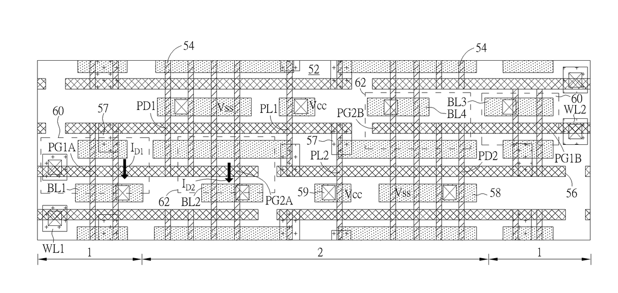
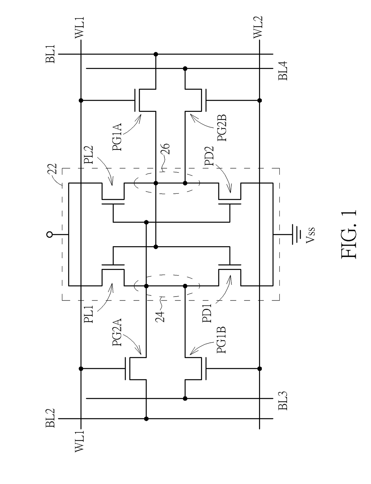
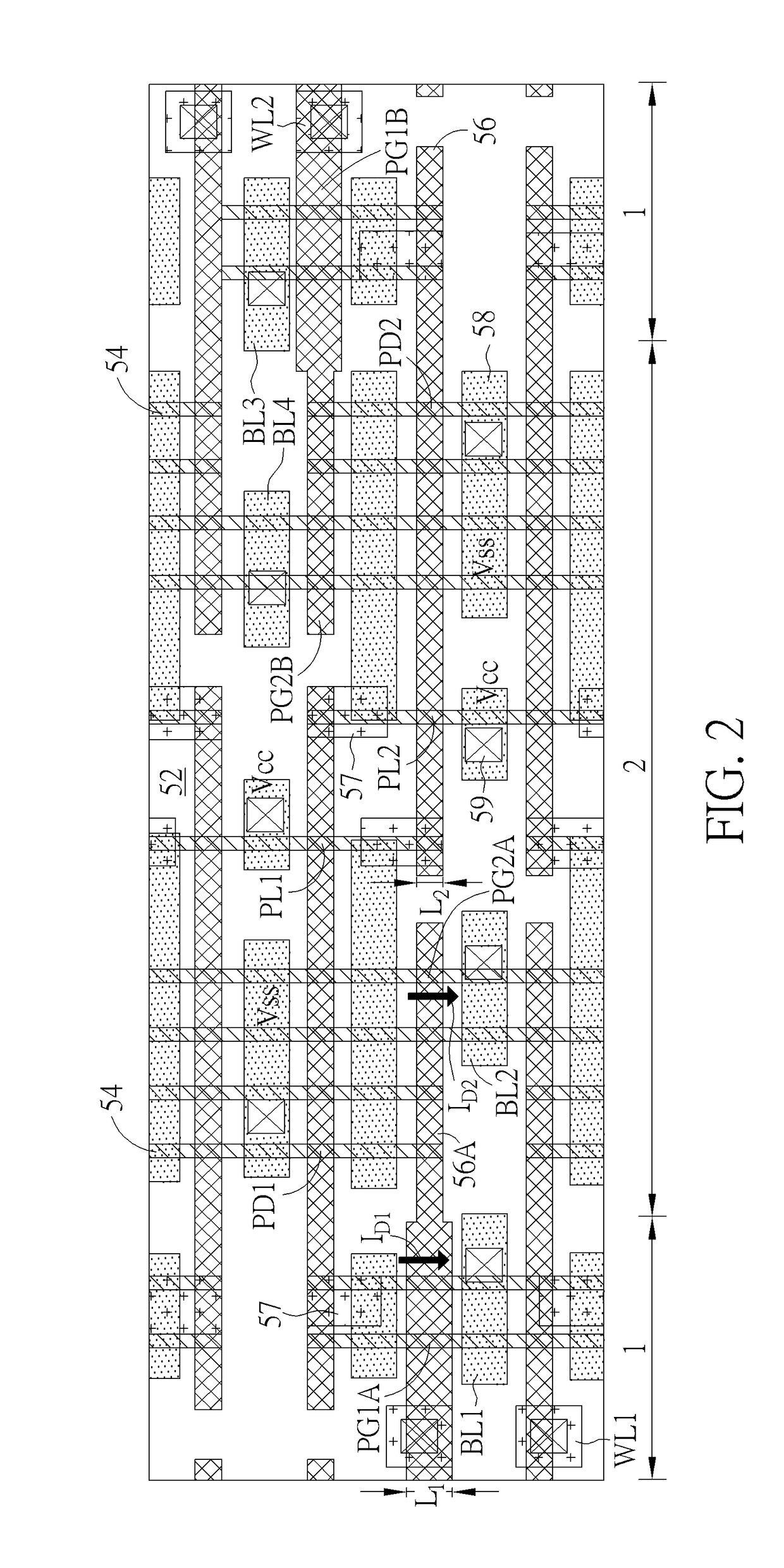
[0018]Referring to FIGS. 1-2, FIG. 1 illustrates a circuit diagram of a SRAM cell according to a fi...


PUM


Abstract

A layout pattern of a static random access memory, including a first inverter and a second inverter constituting a latch circuit. A first inner access transistor, a second inner access transistor, a first outer access transistor and a second outer access transistor are electrically connected to the latch circuit, wherein the first outer access transistor has a first gate length, the first inner access transistor has a second gate length, and the first gate length is different from the second gate length.

Description

BACKGROUND OF THE INVENTION[0001]1. Field of the Invention[0002]The invention relates to a static random access memory (SRAM), and more particularly, to a SRAM having the advantage of decreasing the current differences in different regions.[0003]2. Description of the Prior Art[0004]An embedded static random access memory (SRAM) comprises a logic circuit and a static random access memory connected to the logic circuit. SRAM is a kind of volatile memory cell, which means it preserves data only while power is continuously applied. SRAM is built of cross-coupled inverters that store data during the time that power remains applied, unlike dynamic random access memory (DRAM) that needs to be periodically refreshed. Because of its high access speed, SRAM is also used in computer systems as a cache memory.[0005]However, as pitch of the exposure process decreases, it has been difficult for the current SRAM architecture to produce desirable patterns. Hence, how to enhance the current SRAM arc...

Claims


Application Information

Patent Timeline
IPC IPC(8): H01L27/02G03F1/36G06F17/50G11C11/419
CPCH01L27/0207G06F17/5068G03F1/36G11C11/419G11C11/412H10B10/12G06F30/39
Inventor WANG, JUN-JIEWANG, YU-LINCHANG, TZU-FENGLEE, WEI-CHI
Owner MARLIN SEMICON LTD
Learn More