Perovskite thin-film photovoltaic cell and preparation method thereof
- Summary
- Abstract
- Description
- Claims
- Application Information
AI Technical Summary
Benefits of technology
Problems solved by technology
Method used
Image
Examples
example 1
[0046]1. The cleaning process of substrate. FTO substrate was cleaned and dried. Firstly, the FTO substrate was cut to a suitable size and cleaned by detergent and washed by deionized water. Secondly, the substrate was washed by an ultrasonic cleaner sequentially in acetone, ethanol, and deionized water. Finally, the substrate was dried by nitrogen gas.
[0047]2. The fabrication of perovskite CH3NH3PbI3 absorber. Firstly, 1 mol / L PbI2 in dimethylformamide was stirred at 60° C. for 12 h. The solution was spin-coated on an FTO substrate without ETL. Secondly, the substrate was soaked into 10 mg / mL CH3NH3I in isopropanol for 5 min and then soaked into clean isopropanol at room temperature. Finally, the film was dried by nitrogen gas and heated in air at 70° C. for 30 min.
[0048]3. The fabrication of HTL. The perovskite film was spin-coated with HTL using a solution composed of 68 mM of spiro-OMeTAD, 26 mM of Li-TFSI, and 55 mM of TBP dissolved in acetonitrile and chlorobenzene (V / V=1:10)....
example 2
[0051]1. The cleaning process of the transparent conductive substrate is the same as Example 1.
[0052]2. The fabrication of TiO2 ETL. To prepare the precursor solution, 0.38 mL of diethanolamine, 1.8 mL of tetrabutyl titanate, and 18 mL of ethanol were stirred at 40° C. for 2 h. To form a sol, the solution should be aged for 24 h. A compact TiO2 film was coated by a spin coating method and then thermally annealed at 550° C. for 30 min.
[0053]3. The fabrication of perovskite CH3NH3PbI3 absorber. Firstly, 1 mol / L PbI2 in dimethylformamide was stirred at 60° C. for 12 h. The solution was spin-coated on an FTO substrate with TiO2 ETL. Secondly, the substrate was soaked into 10 mg / mL CH3NH3I in isopropanol for 5 min and then soaked into clean isopropanol at room temperature. Finally, the film was dried by nitrogen gas and heated in air at 70° C. for 30 min.
[0054]4. The fabrication of HTL is the same as that in Example 1.
[0055]5. The fabrication of electrode is the same as that in Example 1...
example 3
[0057]1. The cleaning process of the transparent conductive substrate is the same as that in Example 1.
[0058]2. The fabrication of SnO2 ETL. 0.025 mol / L SnCl2.2H2O dissolved in ethanol was stirred at room temperature for 30 min. The precursor solution was spin-coated on an ITO substrate and then thermally annealed at 400° C. for 30 min.
[0059]3. The fabrication of perovskite CH3NH3PbI3 absorber. Firstly, 1 mol / L PbI2 in dimethylformamide was stirred at 60° C. for 12 h. The solution was spin-coated on an FTO substrate with SnO2 ETL. Secondly, the substrate was soaked into 10 mg / mL CH3NH3I in isopropanol for 5 min and then soaked into clean isopropanol at room temperature. Finally, the film was dried by nitrogen gas and heated in air at 70° C. for 30 min.
[0060]4. The fabrication of HTL is the same as that in Example 1.
[0061]5. The fabrication of electrode is the same as that in Example 1.
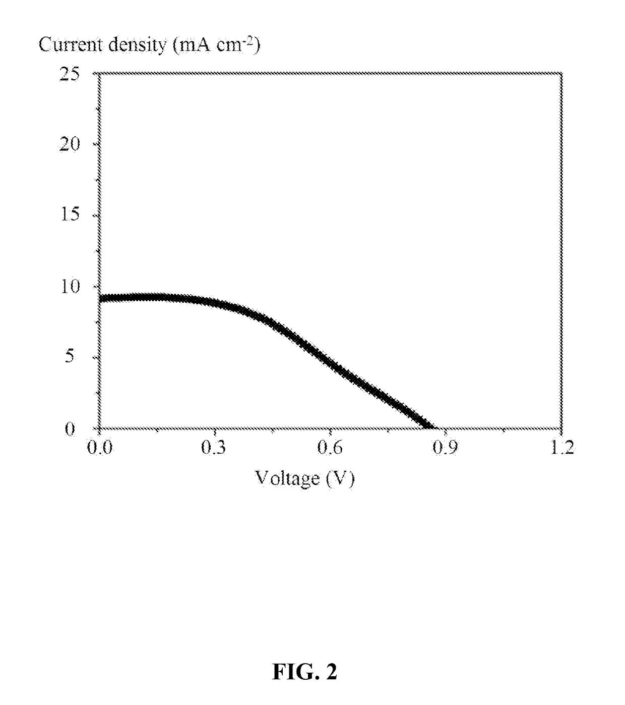
[0062]6. The Test of performance. The device with an active area of 0.09 cm2 was measured under AM1...
PUM
 Abstract
Description
Claims
Application Information
 - R&D
- Intellectual Property
- Life Sciences
- Materials
- Tech Scout
- Unparalleled Data Quality
- Higher Quality Content
- 60% Fewer Hallucinations
Browse by: Latest US Patents, China's latest patents, Technical Efficacy Thesaurus, Application Domain, Technology Topic, Popular Technical Reports.
© 2025 PatSnap. All rights reserved.Legal|Privacy policy|Modern Slavery Act Transparency Statement|Sitemap|About US| Contact US: help@patsnap.com


