
Light source and atomic oscillator

Inactive Publication Date: 2017-04-27
SEIKO EPSON CORP
View PDF2 Cites 0 Cited by
  • Summary
  • Abstract
  • Description
  • Claims
  • Application Information

AI Technical Summary

Benefits of technology

The invention provides a light source that can control its output wavelength and optical output individually. This allows for better control over the light output from the source. The light source also includes an atomic oscillator, which uses this controlled light to generate accurate optical signals. The light source is designed to prevent changes in its output due to changes in temperature, which can lead to fluctuations in the central wavelength of the light. This makes it easier to control the output of the light source and reduces contact resistance between the electrodes.

Problems solved by technology

Therefore, it is necessary to form a control loop of the atomic oscillator in consideration of this, and complicated control is required.

Method used


Image

  • Light source and atomic oscillator
  • Light source and atomic oscillator
  • Light source and atomic oscillator

Examples


first modification example

3.1. First Modification Example

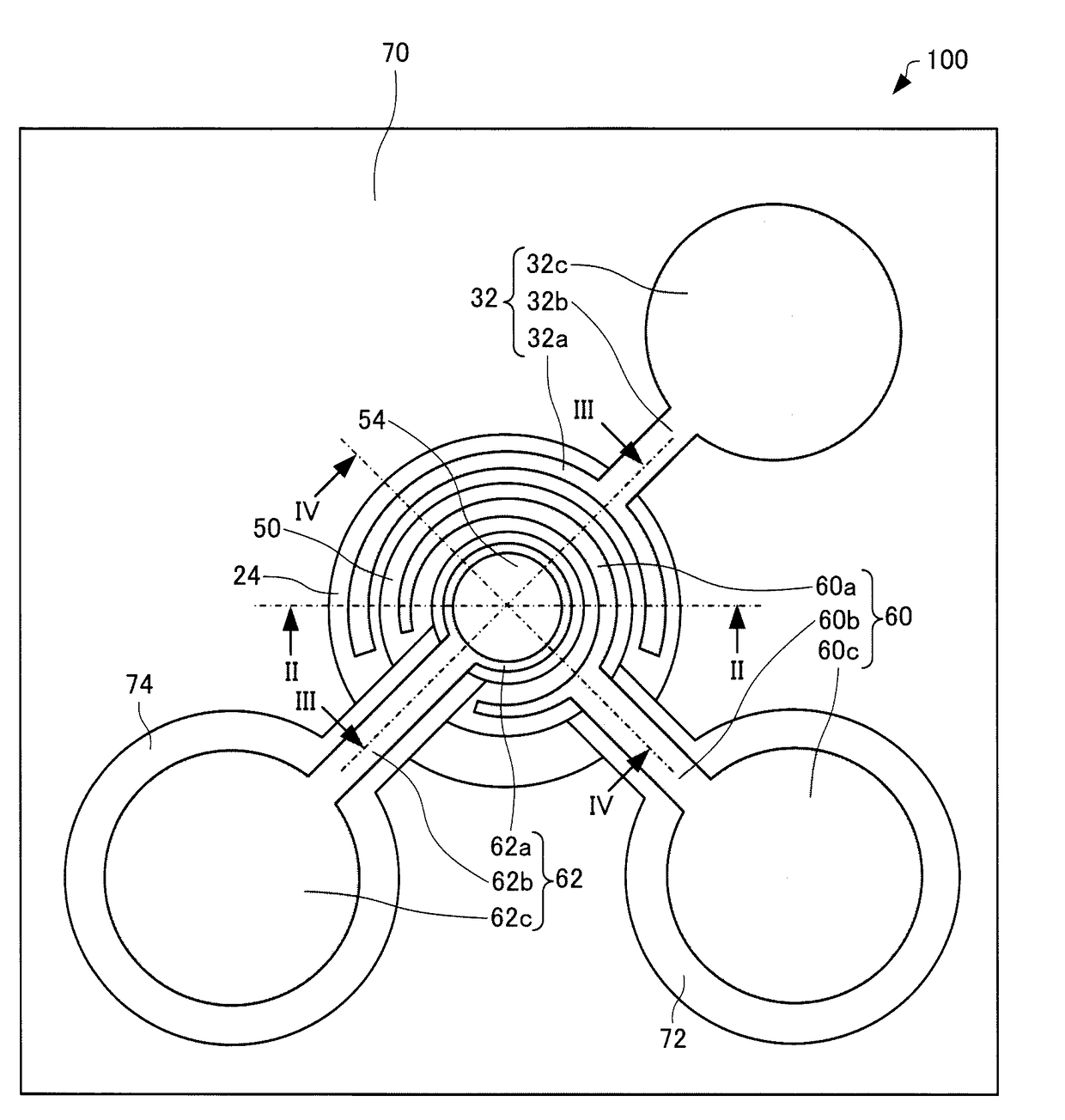
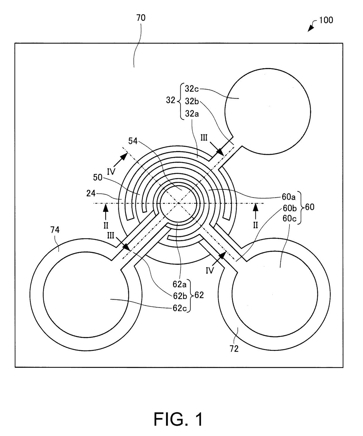
[0081]Next, a light source according to the first modification example of the present embodiment will be described, referring to drawings. FIG. 9 is a sectional view schematically illustrating a light source 200 according to the first modification example of the present embodiment. FIG. 10 is a plan view schematically illustrating the light source 200 according to the first modification example of the present embodiment. It should be noted that illustration of members other than the contacting part 62a of the fourth electrode 62, the first contact layer 50, and the heat insulating layer 40, is omitted in FIG. 10 for convenience.

[0082]Hereinafter, in the light source 200 according to the first modification example of the present embodiment, members having the same functions as those of the constituent members of the light source 100 according to the present embodiment will be designated by the same reference signs, and the detailed description thereof w...

second modification example

3.2. Second Modification Example

[0089]Next, a light source according to a second modification example of the present embodiment will be described, referring to drawings. FIG. 12 is a plan view schematically illustrating a light source 300 according to the second modification example of the present embodiment. FIG. 13 is a sectional view, taken along line XIII-XIII of FIG. 12, schematically illustrating the light source 300 according to the second modification example of the present embodiment.

[0090]The light source 300, as illustrated in FIG. 13, is different from the above-described light source 100 in that the light source 300 has a heat diffusion layer 42.

[0091]The heat diffusion layer 42 is provided on the heat insulating layer 40. The heat diffusion layer 42 is provided between the heat insulating layer 40 and the first contact layer 50. A planar shape of the heat diffusion layer 42 is, for example, circular. In the plan view, the area of the heat diffusion layer 42 and the are...


PUM


Abstract

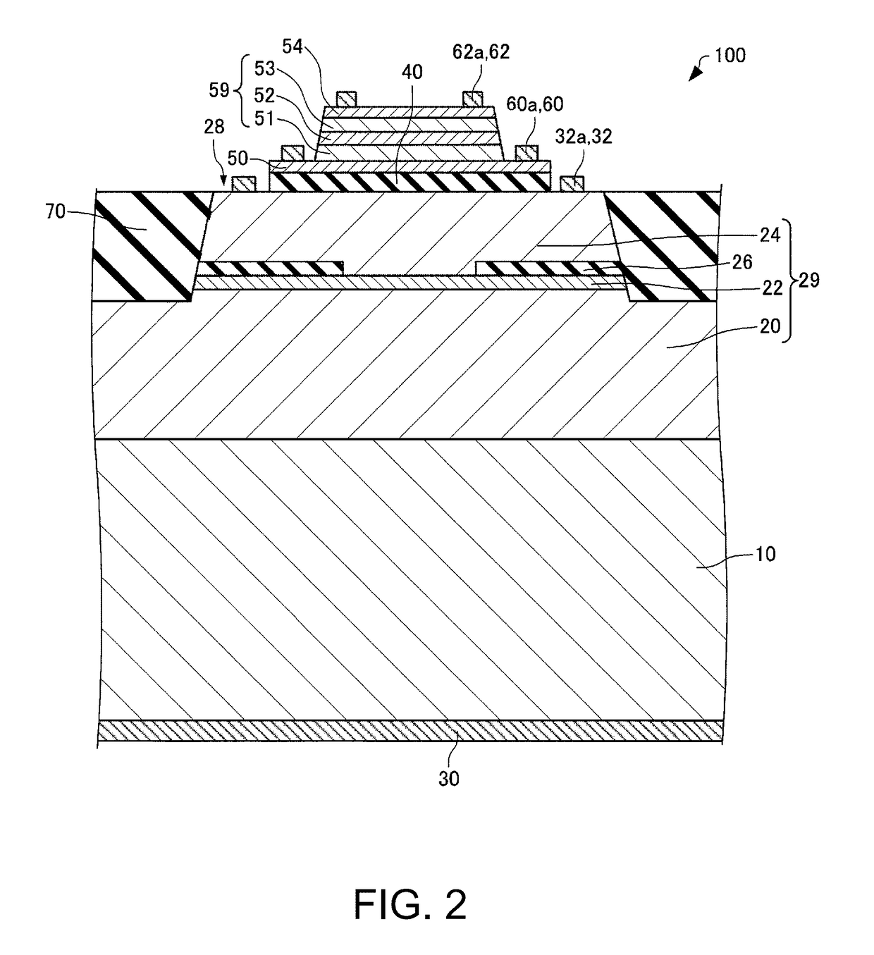
A light source includes an optical oscillation layer having a first reflective layer, an active layer, and a second reflective layer laminated therein in this order; an electrical field absorption layer having a first semiconductor layer, a quantum well layer, and a second semiconductor layer laminated therein in this order; and a heat insulating layer that is disposed between the optical oscillation layer and the electrical field absorption layer and has a lower thermal conductivity than that of the second reflective layer.

Description

BACKGROUND[0001]1. Technical Field[0002]The present invention relates to a light source and an atomic oscillator.[0003]2. Related Art[0004]An atomic oscillators using transition energy of atoms as reference frequency is widely used as one of highest-precision oscillators in communication base stations or the like. Although there are several types as the atomic oscillator, a microwave double resonance type using a rubidium (Rb) lamp is most generally used.[0005]In recent years, an atomic oscillator using a phenomenon called Coherent Population Trapping (CPT) that is one of quantum interference effects is suggested (for example, refer to JP-A-2015-62167), and reduced size and low power consumption of the atomic oscillator are expected compared with the related art. In the case of the CPT type, sidebands are used for development of a CPT phenomenon by superimposing a high-frequency signal using a coherent light source, such as a laser, as a light source. The CPT type atomic oscillator ...

Claims


Application Information

Patent Timeline
IPC IPC(8): H03L7/26H01S5/125H01S5/343H01S5/042H01S5/0687
CPCH03L7/26H01S5/0421H01S5/0425H01S5/34313H01S5/125H01S5/0687H01S5/183H01S5/18302H01S5/18308H01S5/3432H01S2301/176H01S5/04252H01S5/04256
Inventor NISHIDA, TETSUO
Owner SEIKO EPSON CORP
Learn More