
Ion milling device

a technology of a milling device and a surface is applied in the field of ion milling devices and, which can solve the problems of difficult polishing of hard samples, difficult cross-section processing of composite materials, and crushed or deeply scratched surfaces to be observed

Active Publication Date: 2016-06-09
HITACHI HIGH-TECH CORP
View PDF7 Cites 7 Cited by
  • Summary
  • Abstract
  • Description
  • Claims
  • Application Information

AI Technical Summary

Benefits of technology

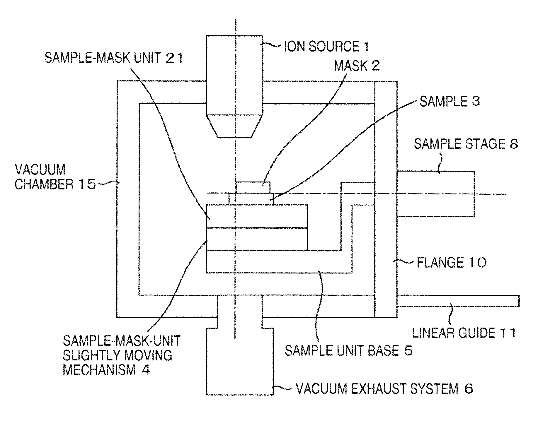
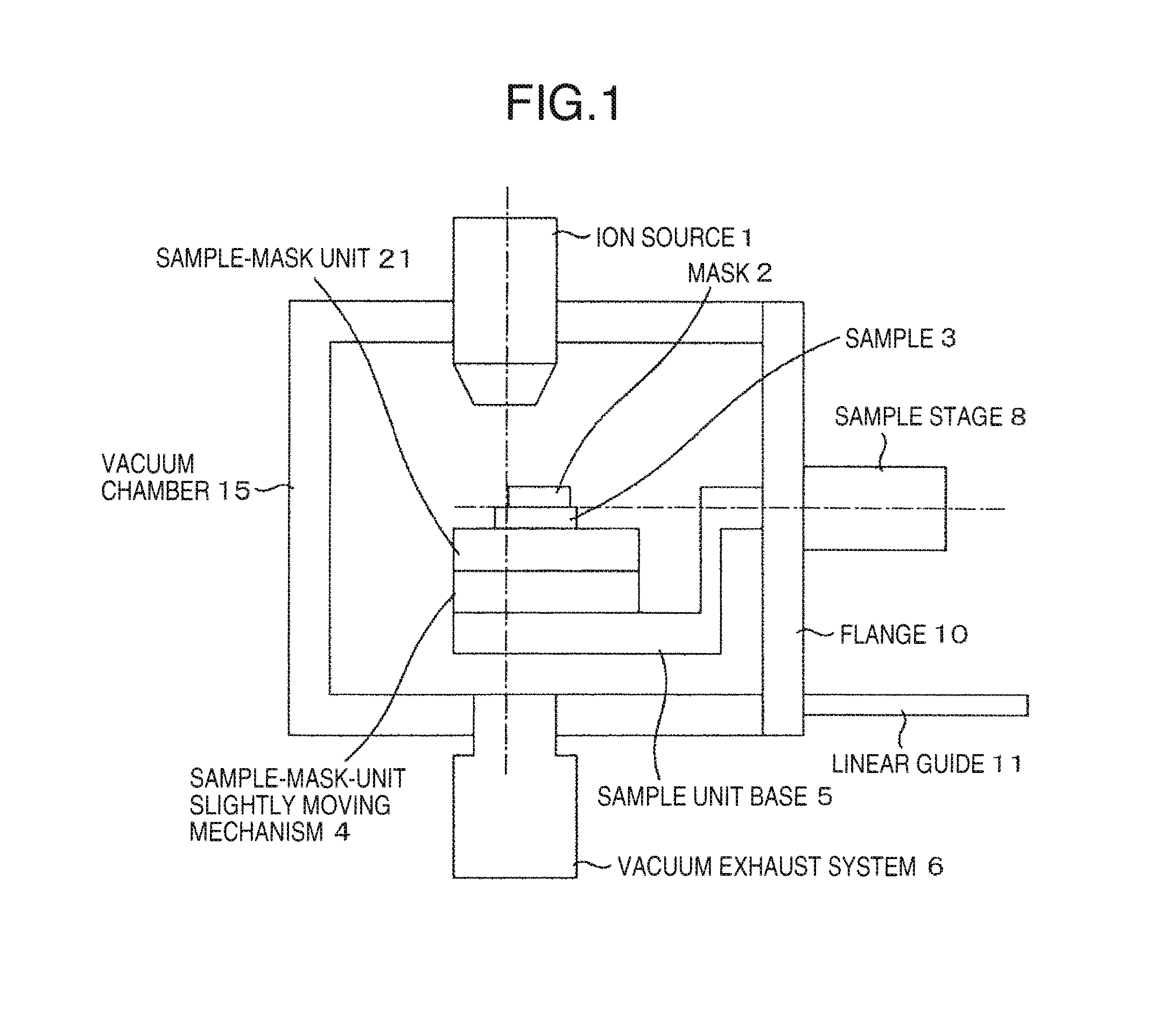
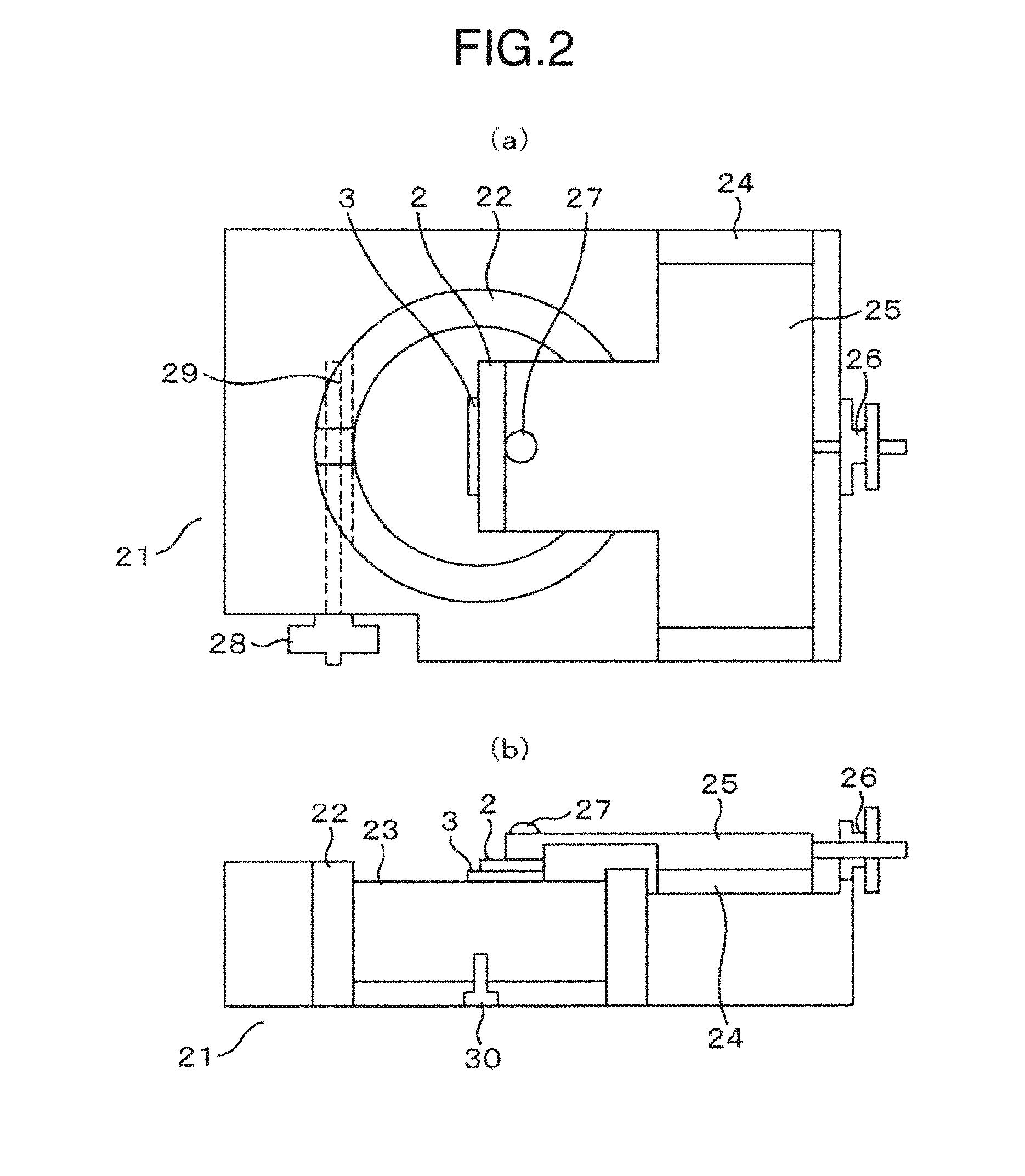
The patent text describes a device that uses ion milling to process samples without damaging their surface. The device can polish hard samples and composite materials. It can also easily obtain a cross section in a mirror state. The text explains that the device includes an ion beam irradiating unit, a tilt stage, a sample holder, and a shielding member. The device changes the tilt angle of the stage to process samples with the ion beam. The technical effect of the device is that it provides a method for soft sample processing without damage, as well as polishing of hard samples and composite materials.

Problems solved by technology

The mechanical polishing has a problem that, when a soft sample such as of a polymer material or aluminum is polished, the surface to be observed is crushed or deeply scratched by particles of an abrasive compound.
Moreover, the mechanical polishing also has problems that it is difficult to polish a hard sample such as of glass or a ceramic and that it is extremely difficult to perform cross-section processing on a composite material in which a soft material and a hard material are stacked.

Method used


Image

  • Ion milling device
  • Ion milling device
  • Ion milling device

Examples


Embodiment Construction

[0036]In a cross-section milling device (device for forming a smooth surface in a sample by milling the sample via a mask), a sample stage and a unit for holding a sample are placed on the same rotation tilt axis (which means they have the same movement). For this reason, a processing observation window is placed on the same axial direction as that of the sample stage. Accordingly, when the sample stage is located on a front surface of the device, the processing observation window is located on the front surface or a rear surface of the device, which makes it difficult to place and operate an observation device (microscope). In addition, flat surface milling (which smoothly flattens a surface perpendicular to an axis of an ion beam (which means the tilt angle of the sample stage is 90 degrees)) cannot be enabled by only replacing a rotating and tilting mechanism of the cross-section milling device with a rotating mechanism; accordingly milling devices respectively for cross-section ...


PUM

PropertyMeasurementUnit
tilt angleaaaaaaaaaa
distanceaaaaaaaaaa

Abstract

An ion milling device of the present invention is provided with a tilt stage (8) which is disposed in a vacuum chamber (15) and has a tilt axis parallel to a first axis orthogonal to an ion beam, a drive mechanism (9, 51) which has a rotation axis and a tilt axis parallel to a second axis orthogonal to the first axis and rotates or tilts a sample (3), and a switching unit which enables switching between a state in which the ion beam is applied while the sample is rotated or swung while the tilt stage is tilted, and a state in which the ion beams is applied while the tilt stage is brought into an untilted state and the sample is swung. Consequently, the ion milling device capable of performing cross-section processing and flat processing of the sample in the same vacuum chamber is implemented.

Description

TECHNICAL FIELD[0001]The present invention relates to an ion milling device and an ion milling method for fabricating a sample to be observed by using a scanning electron microscope (SEM), a transmission electron microscope (TEM), or the like.BACKGROUND ART[0002]An ion milling device is a device for polishing a surface or cross section of a metal, glass, ceramic, or the like by irradiating the surface or cross section with an argon ion beam, and is favorable as a pre-processing device for observation of a surface or cross section of a sample using an electron microscope.[0003]In the conventional cross-sectional observation of a sample using an electron microscope, a vicinity of a part to be observed is first cut by using a diamond cutter, a jigsaw, or the like, for example. Then, after the cut surface is mechanically polished, the sample is placed on a sample table for an electron microscope and the image of the cut surface is observed.[0004]The mechanical polishing has a problem th...

Claims


Application Information

Patent Timeline
Patent Type & Authority Applications(United States)
IPC IPC(8): H01J37/305H01J37/304H01J37/30
CPCH01J37/3053H01J37/3005H01J37/3007H01J2237/26H01J2237/20207H01J2237/20214H01J37/304H01J37/20H01J37/16H01J37/30H01J37/305
Inventor IWAYA, TORUMUTO, HIROBUMITAKASU, HISAYUKIKAMINO, ATSUSHIKANEKO, ASAKO
Owner HITACHI HIGH-TECH CORP
Learn More