Advanced polishing pad materials and formulations
a technology of polishing pads and polishing pads, applied in the field of polishing pads, can solve the problems of non-uniform polishing, high cost and time-consuming, worn or glazed polishing pads,
- Summary
- Abstract
- Description
- Claims
- Application Information
AI Technical Summary
Benefits of technology
Problems solved by technology
Method used
Image
Examples
process examples
Additive Manufacturing Apparatus and Process Examples
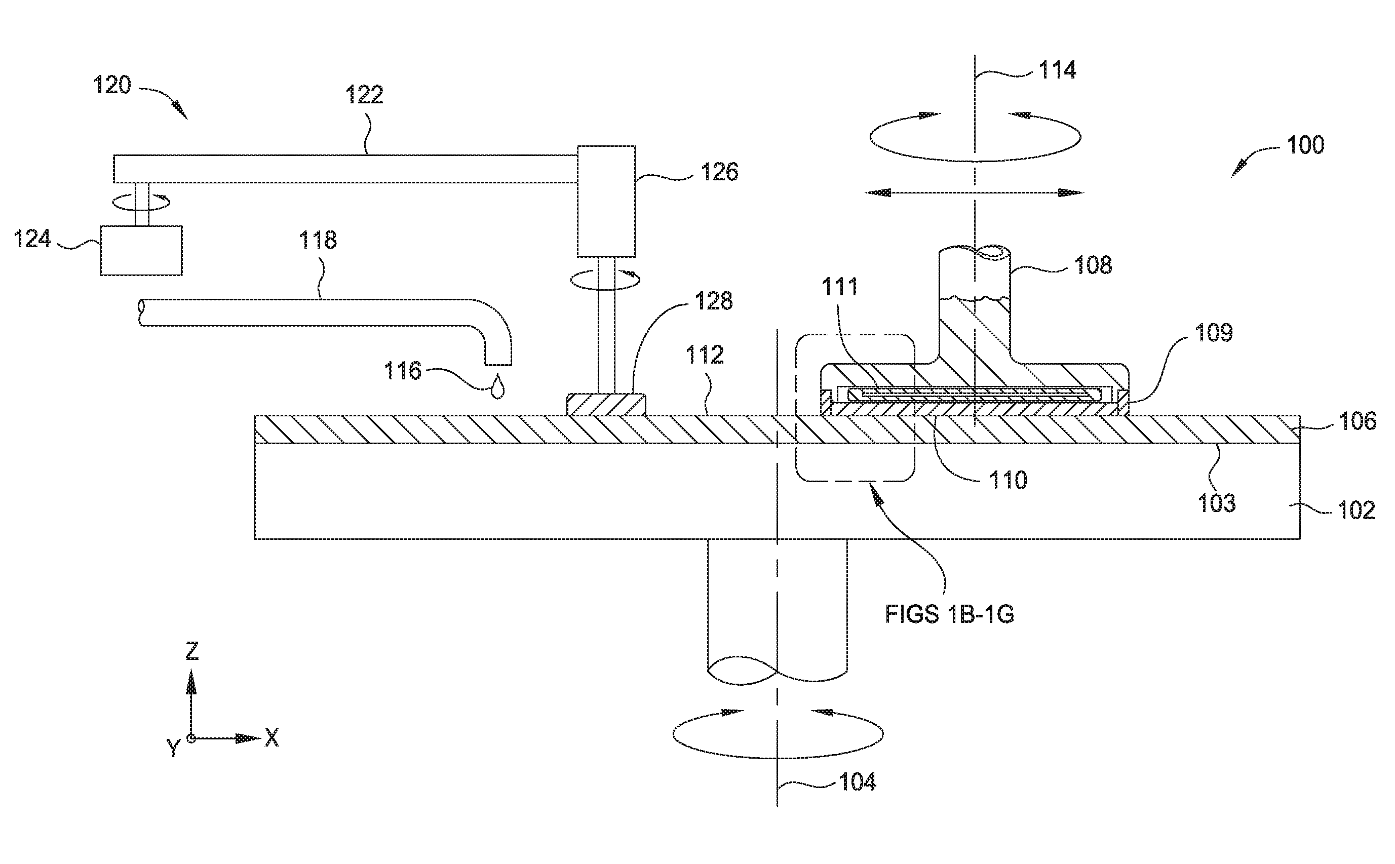
[0088]FIG. 3A is a schematic sectional view of an additive manufacturing system 350 that can be used to form an advanced polishing pad using an additive manufacturing process according to one or more embodiments of the present disclosure. An additive manufacturing process may include, but are not limited to a process, such as a polyjet deposition process, inkjet printing process, fused deposition modeling process, binder jetting process, powder bed fusion process, selective laser sintering process, stereolithography process, vat photopolymerization digital light processing, sheet lamination process, directed energy deposition process, or other similar 3D deposition process.
[0089]The additive manufacturing system 350 generally includes a precursor delivery section 353, a precursor formulation section 354 and a deposition section 355. The deposition section 355 will generally include an additive manufacturing device, or hereafter pr...
process example
Advance Polishing Pad Formation Process Example
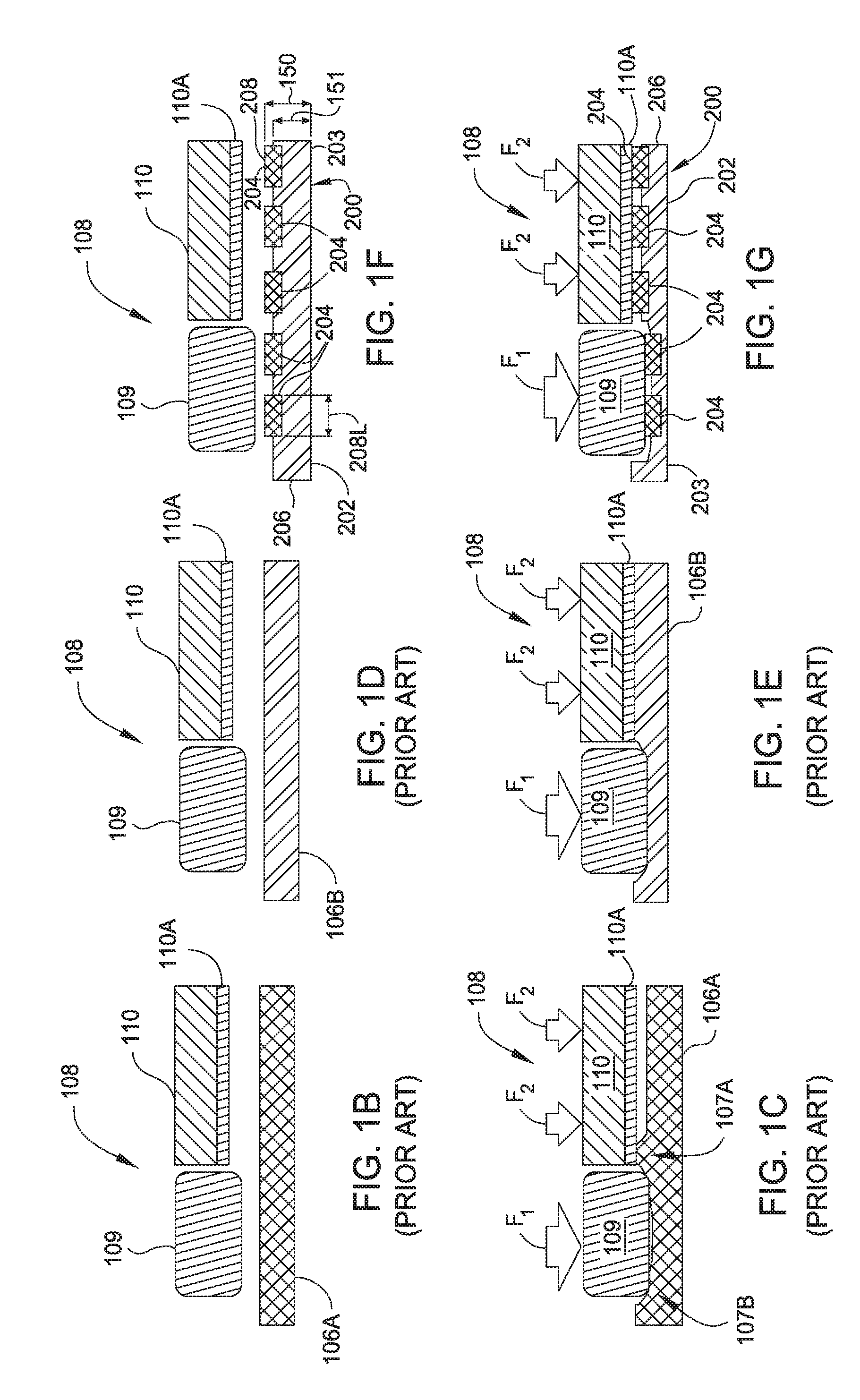
[0117]In some embodiments, the construction of an advanced polishing pad 200 begins by creating a CAD model of the polishing pad design. This can be done through the use of existing CAD design software, such as Unigraphics or other similar software. An output file, which is generated by the modelling software, is then loaded to an analysis program to ensure that the advanced polishing pad design meets the design requirements (e.g., water tight, mass density). The output file is then rendered, and the 3D model is then “sliced” into a series of 2D data bitmaps, or pixel charts. As noted above, the 2D bitmaps, or pixel charts, are used to define the locations across an X and Y plane where the layers in the advanced polishing pad will be built. In some additive manufacturing process applications these locations will define where a laser will pulse, and in other applications the location where a nozzle will eject a droplet of a material.
[011...
example 1
Storage Modulus E′ and E′30:E′90 Ratio Control Example
[0155]The selection, formulation and / or formation of materials that have a desirable storage modulus E′ and E′30:E′90 ratio in desirable regions of an advanced polishing pad by use of an additive manufacturing process is an important factor in assuring that the polishing results achieved by the advanced polishing pad are uniform across a substrate. It is noted that storage modulus E′ is an intrinsic material property of a formed material, which results from the chemical bonding within a cured polymeric material. Storage modulus may be measured at a desired temperature, such as 30° C. and 90° C. using a dynamic mechanical analysis (DMA) technique. Examples of formulations that contain different storage moduli are illustrated below in Table 4.
TABLE 4ItemMaterial CompositionFormulationE′30E′90No.(See Table 3 Ref. Name)Composition (wt %)(MPa)(MPa)E′30 / E′901O1:M345:554043.6113.62O1:M145:551595169.59.43O1:M3:M1:M245:22:22:1168010.465.3...
PUM
 Abstract
Description
Claims
Application Information
 - R&D
- Intellectual Property
- Life Sciences
- Materials
- Tech Scout
- Unparalleled Data Quality
- Higher Quality Content
- 60% Fewer Hallucinations
Browse by: Latest US Patents, China's latest patents, Technical Efficacy Thesaurus, Application Domain, Technology Topic, Popular Technical Reports.
© 2025 PatSnap. All rights reserved.Legal|Privacy policy|Modern Slavery Act Transparency Statement|Sitemap|About US| Contact US: help@patsnap.com


