Pressure sensing implant

Active Publication Date: 2016-02-04
ENDOTRONIX
View PDF6 Cites 39 Cited by
  • Summary
  • Abstract
  • Description
  • Claims
  • Application Information

AI Technical Summary

Benefits of technology

This patent describes a design for a wireless circuit that is designed to be implanted in a person's body. The goal is to make the circuit easy to manufacture, small in size, long-lasting, and have good RF characteristics. One way to achieve this is by using a housing with at least one thin wall that is hermetically sealed. The housing contains an antenna coil that is parallel to the thin wall. The circuit can also have a sensor with conductive features that are patterned in a solid area and can include breaks or slots. The sensor can be connected to the housing at an opening in the housing. Overall, the design of the circuit allows for a small form factor and optimal RF quality factor.

Problems solved by technology

However, there are many tradeoffs and design constraints in designing such implantable sensors, such as size, cost and manufacturability.
A key challenge in successful commercialization of these implantable wireless sensors is the design tradeoff between implant size and the “link distance”, which is the physical distance between the implant and the external device communicating with the implant.
However, from a wireless communication standpoint, the smaller the implant, the shorter the link distance.
This distance limitation is driven primarily by the size of the antenna that can be realized for a given overall implant size.
This increase in flux through the implant antenna can result in an increase in link distance.
An additional challenge arises due to regulatory policies and licensed frequency bands for commercial use.
With current technology, it is difficult to reliably fabricate an accurate ultra-miniature implantable wireless pressure sensor with high quality factor at low operating frequencies within a tightly controlled operating range.
While an ultra-miniature sensor requires an inductor with high Q to ensure reliable wireless signal communication at appropriate distance between sensor and external device, a high Q inductor places limitations on overall sensor size.
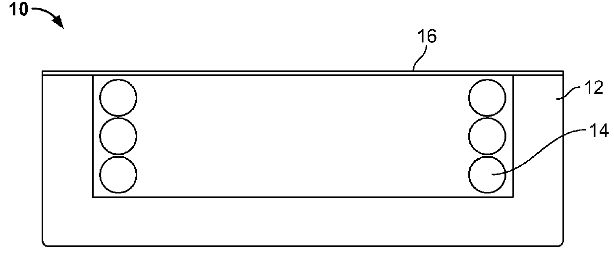
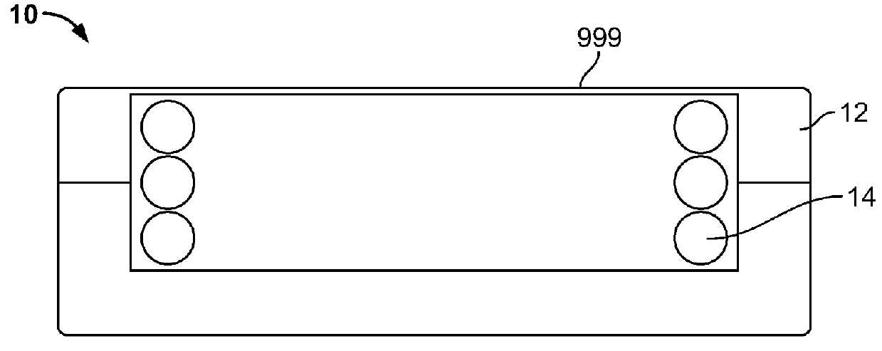
Furthermore, placement of the capacitor 12 near the inner turns of the inductor spiral coil 14 may also significantly reduce the quality factor of the LC sensor.
Also, placement of the capacitor electrodes on the plane of or near the inductor can reduce the quality factor of the LC sensor.
Thus in known sensors, capacitors are placed adjacent to an inductor, which increases the size of the sensor, or inside the central area of the spiral inductor with significant space between the inner turns of the spiral inductor and the edges of the capacitor plates, which limits the size of the capacitor and / or the size of the inductor.
Known wireless pressure sensors are also limited by having a capacitive sensor that does not have a high Q. In known implantable pressure sensors, capacitive sensors are realized by large solid area electrodes.
This capacitance design is not optimal and results in a low quality factor capacitance for high frequency alternating currents.
Large solid area electrodes of a capacitor when not positioned away from the inductor result in reduced quality factor of an LC circuit due to eddy currents in the capacitor electrode when the electrode is subject to high frequency alternating currents.
There are further challenges with known sensors to realize a sensor that operates within approved frequency ranges for wireless signal transmission and at the same time experiences minimal signal attenuation through the human body.
Both inductance and capacitance are limited by size.
Controllably fabricating electrodes with a small gap within practical manufacturing tolerances is challenging and could result in a lower breakdown voltage between the electrodes, stiction of the electrodes, limited pressure operating range, and low yield or high cost.
In many cases, it is difficult to tightly control the capacitance of a sensor within an economical production environment.
With known LC sensors, the operating range of the passive sensor cannot be modified after fabrication of the device as often both the capacitor and the inductor are sealed from the environment.
Such designs require operation of the devices over larger operating ranges to account for manufacturing tolerances and these ranges may not be approved for commercial use by regulatory bodies.
Other current methods to tune the operating range of a sensor after fabrication requires on chip calibration efforts which can increase the size of the sensor and / or the power consumption of the sensor which reduces the usefulness of the sensor.
With current technology, it is difficult to fabricate a small sensor that can operate in a specified operating range at low frequencies.
Another challenge in commercialization of implantable wireless sensors is the need to protect the sensitive sensor electronics from potentially corrosive or damaging fluids of the body.
Small changes in electrical, chemical, or mechanical properties of the implant over this time period can result in inaccurate measurements.
Unfortunately, the use of metals in hermetic enclosures may negatively impact the ability of the sensor to communicate wirelessly with an external device, especially when communication at low radiofrequencies is desired.
While ceramics and glasses are compatible with wireless RF communication, it is difficult to machine ceramics to a thin walled hermetic enclosure.
Hermetic enclosures known in the art, particularly those made of ceramic and / or glass materials, do not lend themselves to efficient use of limited space.
However, sidewalls of an implant package made with these techniques often require use of a dicing saw or laser to separate the implant package from the remaining substrate.
Due to manufacturing constraints and the need for mechanical strength, implant package sidewalls made by these methods are typically 0.3 mm-0.5 mm thick.
Alternative manufacturing approaches, such as the molding or machining of ceramic, are typically limited to minimum sidewalls of 0.5-0.7 mm thick.
In these architectures, total coil area is limited by the need for a relatively thick structural wall outside the coil perimeter.

Method used


Image

  • Pressure sensing implant
  • Pressure sensing implant
  • Pressure sensing implant

Examples


Embodiment Construction

[0065]Reference will now be made in detail to embodiments of the invention, examples of which are illustrated in the accompanying drawings. It is to be understood that other embodiments may be utilized and structural and functional changes may be made without departing from the respective scope of the invention.

[0066]This application relates to implant packages and more particularly to an implantable sensor design and manufacturing approach to optimize manufacturability, size, longevity, RF characteristics, and overall performance. To facilitate maximum link distance for a given implant size, the enclosure should be constructed to maximize antenna coil area, while still providing ample protection.

[0067]The implant package may utilize thin membrane materials such as glass, quartz, sapphire, fused silica, alumina, titanium, diamond, or other materials known in the art, to increase the space available inside an implant package of a fixed outer size. Whereas in prior art implant package...


PUM


Abstract

A wireless circuit includes a housing having at least one opening, and sensor connected to the housing at the opening. The sensor includes a first layer having a first dimension and a second layer having a second dimension shorter than the first dimension. The second layer may be positioned entirely within the housing and a surface of said first layer may be exposed to an exterior of the housing.

Description

CROSS-REFERENCE TO RELATED APPLICATIONS[0001]This application claims priority to Provisional Patent Application No. 61 / 786,793 entitled “PRESSURE SENSING IMPLANT,” filed on Mar. 15, 2013. This application is a continuation-in-part of U.S. patent application Ser. No. 14 / 129,725 entitled “IMPLANTABLE SENSOR ENCLOSURE WITH THIN SIDEWALLS,” filed on Dec. 27, 2013, which claims priority to International Patent Application No. PCT / US / 2012 / 044998 entitled “IMPLANTABLE SENSOR ENCLOSURE WITH THIN SIDEWALLS,” filed on Jun. 29, 2012 which claims priority to Provisional Patent Application No. 61 / 502,982 entitled “IMPLANTABLE SENSOR ENCLOSURE WITH THIN SIDEWALLS,” filed on Jun. 30, 2011, each of which are hereby incorporated by reference in its entiretyFIELD OF INVENTION[0002]This application relates to implant packages and more particularly to an implantable sensor enclosure for optimal wireless communication.BACKGROUND[0003]Implantable wireless sensors are useful in assisting diagnosis and tre...

Claims


Application Information

Patent Timeline
IPC IPC(8): A61B5/00A61B5/0215A61B5/07
CPCA61B5/686A61B5/0215A61B2562/168A61B2562/16A61B2562/0247A61B5/076G01L19/0618G01L9/0042B81C2203/0109H05K2201/10151H05K9/0024H05K2201/10371B81B3/0035G01L19/0038B81C1/00261B81B2201/0264B81C2203/0118B81C2203/019B81C2203/075
Inventor ROWLAND, HARRYNAGY, MICHAELWATKINS, ROGERSUNDARAM, BALAMURUGANSUNDARAM, SURESH
Owner ENDOTRONIX
Why Eureka
Try Eureka