Air Gap Creation In Electronic Devices

a technology of electronic devices and air gaps, applied in the direction of waveguides, waveguide type devices, printed element electric connection formation, etc., can solve the problems of limited performance of passive electronic components fabricated on ceramic substrates, increasing the performance of passive electronic components, and meeting continuous technological demands

Inactive Publication Date: 2015-12-03
AEAD HATEM MOHAMED
View PDF5 Cites 7 Cited by
  • Summary
  • Abstract
  • Description
  • Claims
  • Application Information

AI Technical Summary

Benefits of technology

The patent describes a method for creating an air gap in an electronic device to reduce the dielectric constant, which can improve its performance for high frequency microwave transmission. This method allows for the creation of a suspended substrate-like environment by selecting and creating a configurable location for the air gap on the substrate. The air gap can help to reduce capacitance, loss tangent, and electromagnetic fields while also creating a wider strip dimension and more tolerance in the device. This method is cost-effective and efficient for designing high power, high frequency, and wide bandwidth passive electronic component chips with air gaps.

Problems solved by technology

The aforementioned problems associated with ceramic substrates preclude a design engineer from increasing performance of passive electronic components fabricated on ceramic substrates, and from meeting continuous technological demands.
Hence, the passive electronic components fabricated on ceramic substrates have a limited performance, for example, in terms of frequency bandwidth, voltage standing wave ratio (VSWR), attenuation, etc.
Different air gap formation techniques have varying degrees of complexity.
However, this method is expensive.
Typically, these air gap formation techniques are expensive.
Hence, there is a long felt but unresolved need for a method for creating an air gap that attains a reduced dielectric constant in a passive electronic component chip configured for high frequency microwave transmission.
Furthermore, there is a need for a cost effective, efficient, and uncomplicated method for designing high power, high frequency, and wide bandwidth passive electronic component chips comprising air gaps.

Method used


Image

  • Air Gap Creation In Electronic Devices
  • Air Gap Creation In Electronic Devices
  • Air Gap Creation In Electronic Devices

Examples


Embodiment Construction

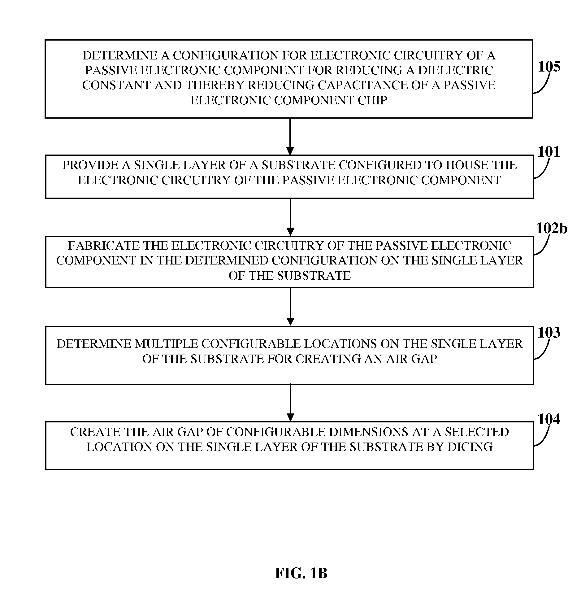
[0092]FIG. 1A illustrates a method for creating an air gap in a passive electronic component chip configured for high frequency microwave transmission. As used herein, “air gap” refers to a space, or a notch, or a groove containing air or a vacuum in a passive electronic component chip. The method disclosed herein relates to manufacturing high power, high frequency, and wide bandwidth passive electronic component products in a chip form that can operate at 50 gigahertz (GHz) and, in an embodiment, above 50 GHz. For example, the method disclosed herein configures resistors in a chip package. An air gap introduced in a substrate of a resistor reduces capacitance of the resistor, thereby making the resistor suitable for operation at high frequencies. In an embodiment, the passive electronic component chips can be standalone chips comprising, for example, one or more input ports and output ports, leads, connector tabs, etc. In another embodiment, the passive electronic component chips c...


PUM

PropertyMeasurementUnit
Dissipation factoraaaaaaaaaa

Abstract

A method for creating an air gap in an electronic device, for example, a passive electronic component chip (PECC) for high frequency microwave transmission is provided. Electronic circuitry of a passive electronic component, for example, a termination, an attenuator, etc., is fabricated in a predetermined configuration on a single layer of a substrate to create the PECC. An air gap of configurable dimensions is created at a configurable location on the substrate by dicing the substrate at the configurable location to create a suspended substrate-like environment in the PECC. The created air gap reduces the dielectric constant at the configurable location and reduces capacitance of the substrate along areas located directly above the air gap. The created air gap also reduces a loss tangent, high frequency attenuation, and electromagnetic fields near a ground plane of the PECC, creates a wide strip dimension, and creates less stringent tolerance in the PECC.

Description

BACKGROUND[0001]Conventional methods for designing high power, high frequency, and wide bandwidth electronic devices, for example, passive electronic components such as terminations, attenuators, resistors, power dividers, directional couplers, filters, etc., use high thermal conductivity ceramic substrates made of materials, for example, alumina, beryllium oxide (BeO), aluminum nitride (AlN), etc. However, the materials used in ceramic substrates have relatively high dielectric constants. The dielectric constant of a material, also referred to as “relative permittivity”, is a ratio of an amount of electrical energy stored in a material by an applied voltage, relative to an amount of electrical energy stored in a vacuum. The dielectric constant of a material is also a ratio of capacitance of a capacitor using the material as a dielectric, compared to a similar capacitor that has a vacuum as its dielectric.[0002]Ceramic substrate materials are typically capacitive materials with high...

Claims


Application Information

Patent Timeline
IPC IPC(8): H01P3/08H05K3/30H05K3/40H05K1/03H05K3/00
CPCH01P3/08H05K1/0306Y10T29/49018H05K3/4038H05K3/30H05K3/0044H01P5/12H01P5/185H01P11/003H05K1/0243H05K2201/10022H05K2201/1006
Inventor AEAD, HATEM MOHAMED
Owner AEAD HATEM MOHAMED
Why Eureka
Try Eureka