
Polyphenylene oligomers and polymers

a polyphenylene and polymer technology, applied in the field of polyphenylene oligomers and polymers, can solve the problems of poor planarization and gap filling properties of polyimides, circuit corrosion, and present challenges to process integration during fabrication, and achieve low dielectric constant, high glass transition temperature, and high thermal stability

Inactive Publication Date: 2001-09-11
THE DOW CHEM CO
View PDF12 Cites 124 Cited by
  • Summary
  • Abstract
  • Description
  • Claims
  • Application Information

AI Technical Summary

Benefits of technology

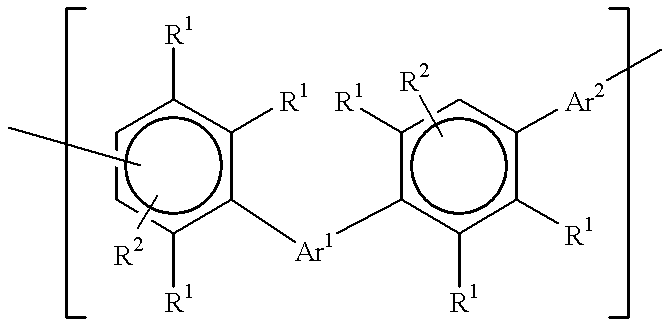
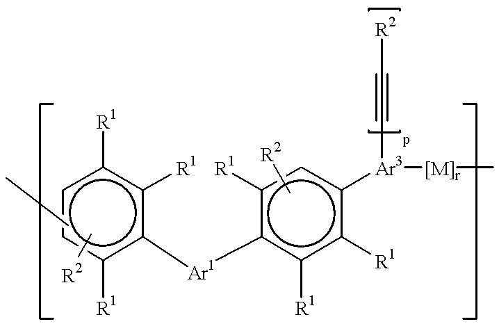
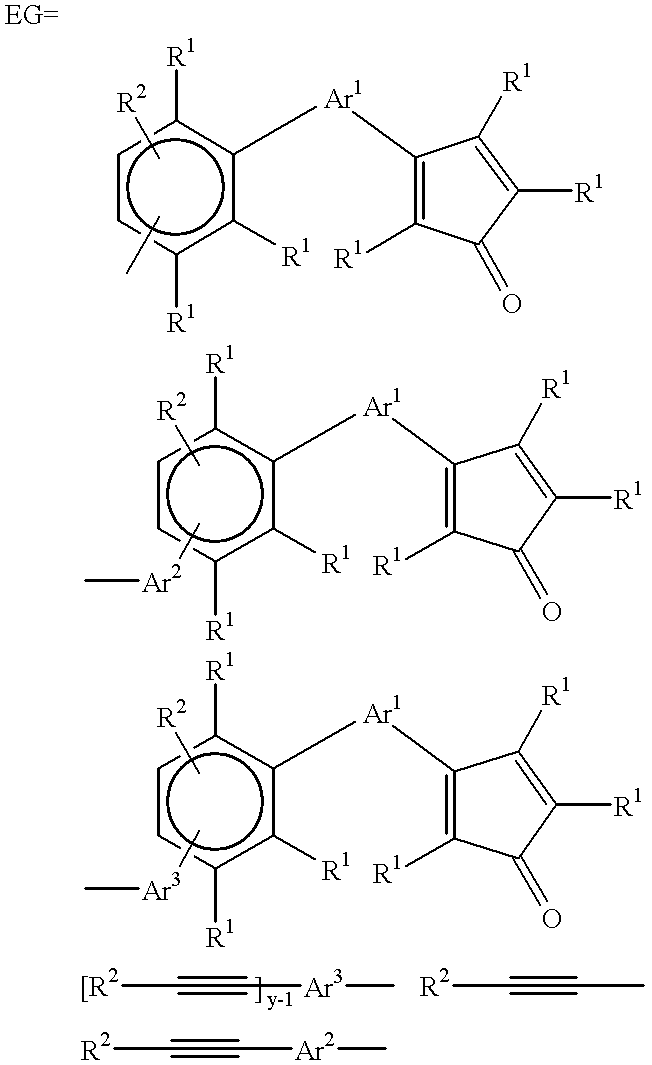
A feature of the invention is that it comprises the reaction product of one or more polyfunctional compounds containing two or more cyclopentadienone groups and at least one polyfunctional compound containing two or more aromatic acetylene groups wherein at least some of the polyfunctional compounds contain three or more reactive groups. An advantage of such a reaction product is that it may gap fill and planarize patterned surfaces, and as cured have high thermal stability, a high glass transition temperature and a low dielectric constant.
Representative examples of such adhesion promoting materials are silanes, preferably organosilanes such as trimethoxyvinylsilane, triethoxyvinylsilane, hexamethyldisilazane [(CH.sub.3).sub.3 --Si--NH--Si(CH.sub.3).sub.3 ], or an aminosilane coupler such as .gamma.-aminopropyltriethoxysilane, or a chelate such as aluminum monoethylacetoacetatediisopropylate [((isoC.sub.3 H.sub.7 O).sub.2 Al(OCOC.sub.2 H.sub.5 CHCOCH.sub.3))]. In some cases, the adhesion promoter is applied from 0.01 weight percent to 5 weight percent solution, excess solution is removed, and then the polyphenylene applied. In other cases, for example, a chelate of aluminum monoethylacetoacetatedi-isopropylate, can be incorporated onto a substrate by spreading a toluene solution of the chelate on a substrate and then baking the coated substrate at 350.degree. C. for 30 minutes in oxygen to form a very thin (for example 5 nanometer) adhesion promoting layer of aluminum oxide on the surface. Other means for depositing aluminum oxide are likewise suitable. Alternatively, the adhesion promoter, in an amount of, for example, from 0.05 weight percent to 5 weight percent based on the weight of the monomer, can be blended with the monomer before polymerization, negating the need for formation of an additional layer.

Problems solved by technology

While polymer dielectrics often provide lower dielectric constants than inorganic dielectrics such as silicon dioxide, they often present challenges to process integration during fabrication.
However, polyimide resins may absorb water and hydrolyze which can lead to circuit corrosion.
Polyimides may exhibit poor planarization and gap fill properties.
Non-fluorinated polyimides may exhibit undesirably high dielectric constants.
The materials described in Kumar and Wrasidlo are soluble but may not be suitable for some uses such as spin coating to fill gaps because the materials were polymerized to exhaustion of the cyclopentadienone moieties which provides relatively high molecular weights.
The molecular weight may be too high to permit application by spin coating over a patterned surface containing gaps to be filled by the dielectric.
Based on the reported glass transition temperatures, such materials may not be able to withstand the processing desired for interlayer dielectrics in integrated circuits.

Method used


Image

  • Polyphenylene oligomers and polymers
  • Polyphenylene oligomers and polymers
  • Polyphenylene oligomers and polymers

Examples


example 2

Preparation of Polymer from Compound M and a Mixture of 1,3-bis(phenylethynyl)benzene (Compound O) and 1,3,5-tris(phenylethynyl)benzene (Compound G)

Compound (M) (316 mg, FW=762, 0.415 mmol), Compound (O) (72 mg, FW=278, 0.259 mmol) and Compound (G) (44 mg, 0.116 mmol) are refluxed in 1,3-diisopropylbenzene (4 mL) for 42 hours. The dark solution turns red and becomes viscous. The solution is spin-coated on a wafer and cured at 400.degree. C. for 1 hour, forming a film. The reaction scheme is as follows: ##STR19##

example 3

Preparation of Polymer from Compound M and a Mixture of 4,4'-bis(phenylethynyl)-o-terphenyl (Compound I) and 4,4',4"-tris(phenylethynyl)-o-terphenyl (Compound N)

Compound (M) (316 mg, 0.415 mmol), Compound (I) (107 mg, FW=430, 0.249 mmol) and Compound (N) (88 mg, FW=530, 0.166 mmol) are refluxed in 5 mL of 1,3-diisopropylbenzene for 48 hours. The yellow viscous solution is cooled to room temperature and spin-coated on a wafer. The polymer is cured at 400.degree. C. for 1 hour, forming a film. The reaction scheme is as follows: ##STR20## ##STR21##

example 4

Preparation of Polymer from 3,3'-(oxydi-1,4-phenylene)bis(2,4,5-triphenylcyclopentadienone) (Compound K) and 4,4'-Bis(phenylethynyl) Diphenyl Ether (Compound H)

3,3'-(Oxydi-1,4-phenylene)bis(2,4,5-triphenylcyclopentadienone) (15.0000 g, 0.019158 mol), 4,4'-bis(phenylethynyl)diphenyl ether (7.0974 g, 0.019158 mol), and N-methylpyrrolidinone (51.60 g) are added to a 250-mL round bottom flask. The flask is attached to a nitrogen inlet and the magnetically stirred solution is heated to 200.degree. C. in an oil bath. After 19.5 hours at 200.degree. C., gel permeation chromatography indicates a M.sub.n of 1551 and a M.sub.w of 2383 relative to a polystyrene standard. The solution is allowed to cool and is bottled. A portion of the solution is taken up in a syringe and filtered through a 1.0 micron syringe filter onto a 4" silicon wafer. The wafer is spin-coated at 2000 rpm for 60 seconds under a heat lamp which warms the wafer. The coated wafer is then placed on a hot plate set to 90.degre...


PUM

PropertyMeasurementUnit
melting pointsaaaaaaaaaa
thicknessaaaaaaaaaa
thicknessaaaaaaaaaa

Abstract

An oligomer, uncured polymer or cured polymer comprising the reaction product of one or more polyfunctional compounds containing two or more cyclopentadienone groups and at least one polyfunctional compound containing two or more aromatic acetylene groups wherein at least some of the polyfunctional compounds contain three or more reactive groups. Such oligomers and uncured polymers may be cured to form cured polymers which are useful as dielectrics in the microelectronics industry, especially for dielectrics in integrated circuits.

Description

This invention relates to polyphenylene oligomers and polymers and processes for preparing and using the same. Such oligomers and polymers may be useful as dielectric resins in microelectronics fabrication.Polymer dielectrics may be used as insulating layers between various circuits and layers within circuits in microelectronic devices such as integrated circuits, multichip modules, laminated circuit boards and the like. The microelectronics fabrication industry is moving toward smaller geometries in its devices to enable lower power and faster speeds. As the conductor lines become finer and more closely packed, the requirements of the dielectrics between such conductors become more stringent.While polymer dielectrics often provide lower dielectric constants than inorganic dielectrics such as silicon dioxide, they often present challenges to process integration during fabrication. For example, to replace silicon dioxide as a dielectric in integrated circuits, the dielectric must be ...

Claims


Application Information

Patent Timeline
Patent Type & Authority Patents(United States)
IPC IPC(8): C08G61/10C08G61/00
CPCC08G61/10C08G2261/312
Inventor GODSCHALX, JAMES P.ROMER, DUANE R.LYSENKO, ZENONMILLS, MICHAEL E.
Owner THE DOW CHEM CO
Learn More