Method of manufacturing mosfet

a manufacturing method and technology of mosfet, applied in the direction of basic electric elements, electrical apparatus, semiconductor devices, etc., can solve the problems of increased junction leakage, increased stress on the channel region, and deterioration of semiconductor materials performance, etc., to achieve the effect of suppressing the edge

Active Publication Date: 2015-10-15
INST OF MICROELECTRONICS CHINESE ACAD OF SCI
View PDF3 Cites 4 Cited by
  • Summary
  • Abstract
  • Description
  • Claims
  • Application Information

AI Technical Summary

Benefits of technology

[0017]According to this method, stress can be applied to a channel region in the semiconductor substrate by the source region and the drain region made of the semiconductor layer. Since the bottom surface and sidewalls of the opening is taken as the growth seed layer during the epitaxial growth, the semiconductor layer may fill up the opening in the semiconductor substrate completely. The semiconductor layer may have a {1 1 1} facet only present in a subsequently grown portion thereof, thereby suppressing the edge effect.

Problems solved by technology

However, the performance of semiconductor materials (e.g., carrier mobility) and the performance of the MOSFETs (e.g., threshold voltage) may also deteriorate as the size of the MOSFETs decreases.
However, the small facets of the semiconductor layer 106 are not desirable because they cause more free surfaces, which release stress from the semiconductor layer 106, thereby reducing the stress applied to the channel region.
However, the silicidation in the semiconductor substrate 101 is undesirable because it may form the metal silicide in a junction region, which leads to increased junction leakage.

Method used


Image

  • Method of manufacturing mosfet
  • Method of manufacturing mosfet
  • Method of manufacturing mosfet

Examples


Embodiment Construction

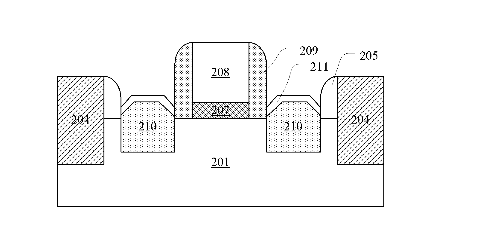
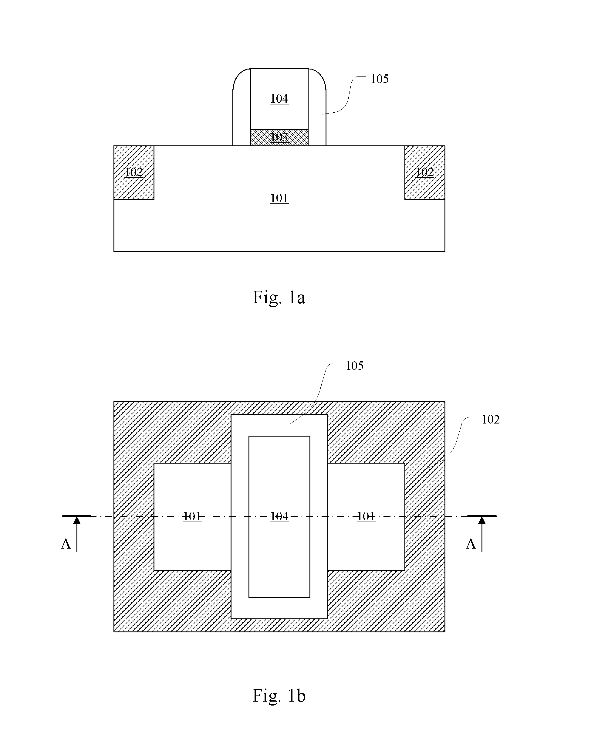
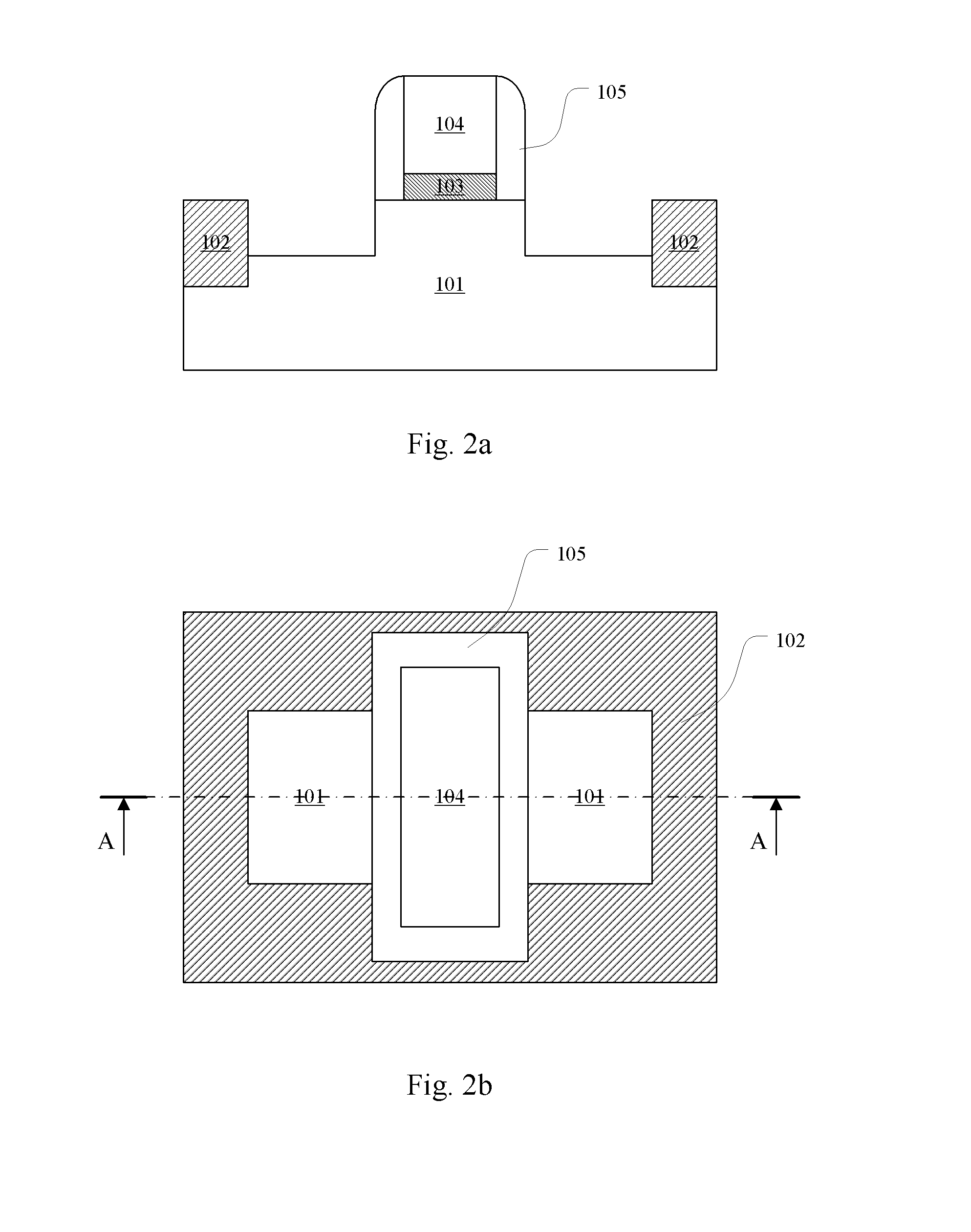
[0020]Exemplary embodiments of the present disclosure are described in detail below with reference to the accompanying drawings. In the drawings, like reference numerals denote like elements. The figures are not necessarily drawn to scale, for the sake of clarity.

[0021]A semiconductor structure obtained by several steps may be illustrated in one figure, for the sake of conciseness.

[0022]In descriptions of structures, when one layer or region is referred to as being “above” or “on” another layer or region, it can be directly above or on the other layer or region, or other layer(s) or region(s) may be arranged there between. Moreover, if the structure in the figures is turned over, the layer or region will be “under” or “below” the other layer or region.

[0023]In order to illustrate a situation in which one layer or region is directly on another layer or region, expressions such as “directly on” or “on and adjoining” may be utilized.

[0024]In the present disclosure, the term “semiconduc...


PUM


Abstract

Provided is a method for manufacturing a MOSFET, including: forming a shallow trench isolation (STI) in a semiconductor substrate to define an active region for the MOSFET; performing etching with the STI as a mask, to expose a surface of the semiconductor substrate, and to protrude a portion of the STI with respect to the surface of the semiconductor substrate, resulting in a protruding portion; forming a first spacer on sidewalls of the protruding portion; forming a gate stack on the semiconductor substrate; forming a second spacer surrounding the gate stack; forming openings in the semiconductor substrate with the STI, the gate stack, the first spacer and the second spacer as a mask; epitaxially growing a semiconductor layer with a bottom surface and sidewalls of each of the openings as a growth seed layer; and performing ion implantation into the semiconductor layer to form source and drain regions.

Description

CROSS-REFERENCE TO RELATED APPLICATION(S)[0001]This application claims priority to Chinese Application No.201210407448.6, filed on Oct. 23, 2012, entitled “METHOD FOR MANUFACTURING MOSFET,” which is incorporated herein by reference in its entirety.TECHNICAL FIELD[0002]The present disclosure relates to a method for manufacturing a MOSFET, and in particular, to a method for manufacturing a MOSFET having enhanced stress.BACKGROUND[0003]An important trend in the development of the integrated circuitry technology is scaling down of metal-oxide-semiconductor field effect transistors (MOSFETs) to improve integration level and reduce manufacturing cost. However, the performance of semiconductor materials (e.g., carrier mobility) and the performance of the MOSFETs (e.g., threshold voltage) may also deteriorate as the size of the MOSFETs decreases.[0004]A MOSFET may have increased carrier mobility due to appropriate stress being applied to a channel region thereof, resulting in a reduced ON r...

Claims


Application Information

Patent Timeline
Patent Type & Authority Applications(United States)
IPC IPC(8): H01L29/66H01L29/165H01L29/78H01L21/265H01L21/762H01L29/06H01L21/306H01L21/308H01L29/161H01L21/02
CPCH01L29/66636H01L29/161H01L29/165H01L29/7848H01L21/02381H01L21/02529H01L29/665H01L21/76224H01L29/0653H01L21/30604H01L21/3081H01L29/6656H01L21/26513H01L21/02532H01L21/3083
Inventor YIN, HAIZHOUZHU, HUILONGQIN, CHANGLIANGYIN, HUAXIANG
Owner INST OF MICROELECTRONICS CHINESE ACAD OF SCI
Why Eureka
Try Eureka