Patterning for selective area deposition

Active Publication Date: 2014-12-25
EASTMAN KODAK CO
View PDF3 Cites 20 Cited by
  • Summary
  • Abstract
  • Description
  • Claims
  • Application Information

AI Technical Summary

Benefits of technology

The present invention describes a way to deposit metal oxides or other materials selectively on a moving substrate, such as a web, using a process called atomic layer deposition. A thin layer of polymer is first deposited on the substrate and then a patterned mask is added which removes the polymer in the areas where the inorganic material is to be deposited. An inorganic layer is then deposited on the substrate selectively using this polymer removal process. This invention allows for the creation of patterned thin films on large areas with high precision.

Problems solved by technology
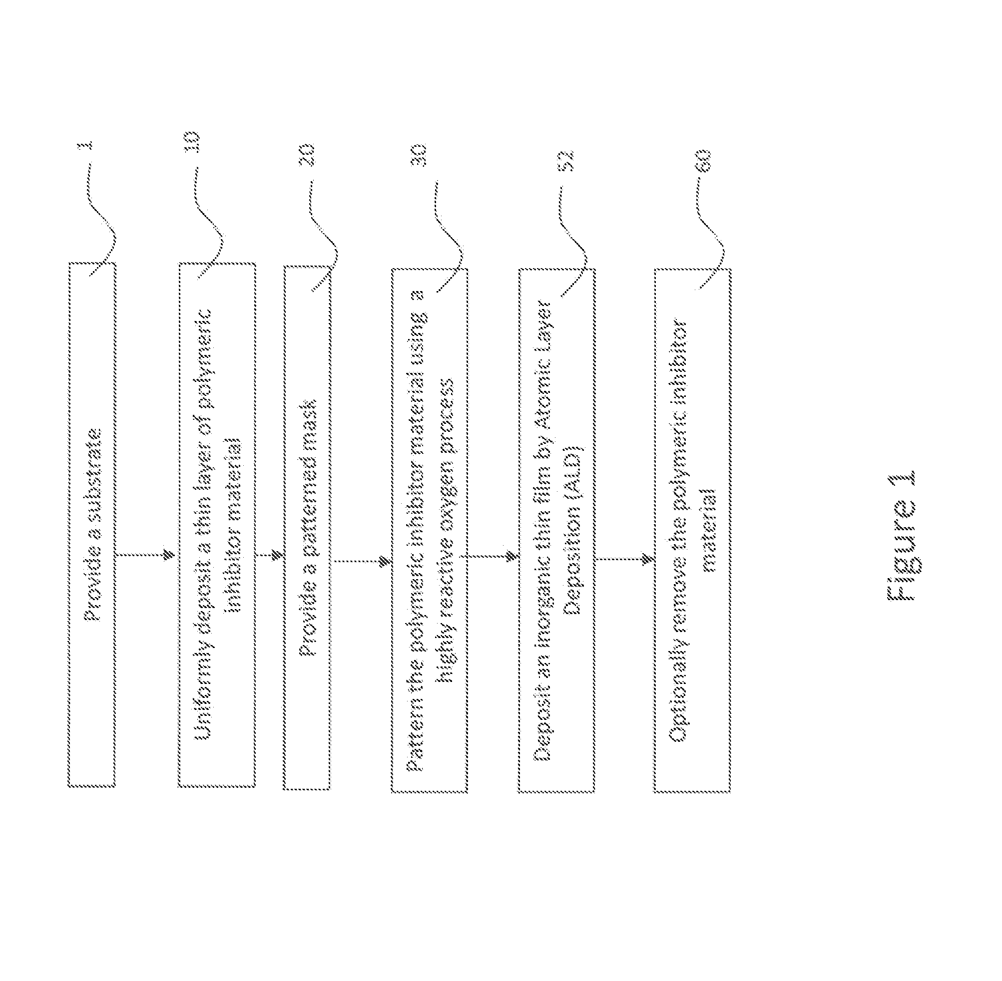
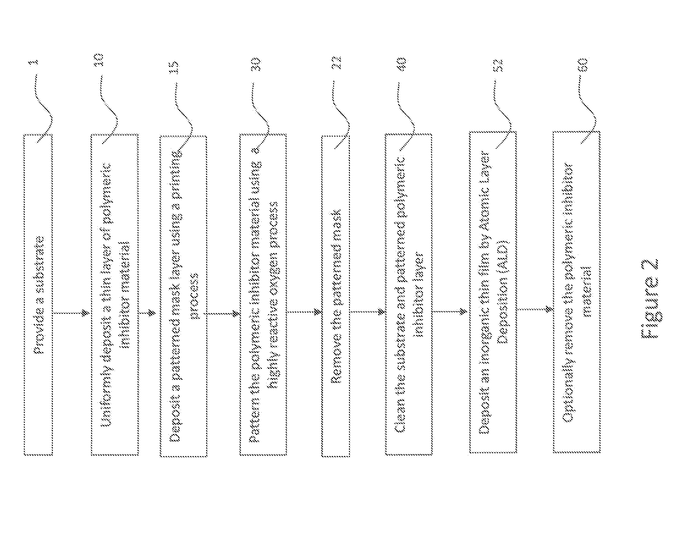
Plastics, however, typically limit device processing to below 200° C. There are other many issues associated with plastic supports when using traditional photolithography during conventional manufacturing, making it difficult to perform alignments of transistor components across typical substrate widths up to one meter or more.
Traditional photolithographic processes and equipment may be seriously impacted by the substrate's maximum process temperature, solvent resistance, dimensional stability, water, and solvent swelling, all key parameters in which plastic supports are typically inferior to glass.
In practice, as in any process, it is difficult to avoid some direct reaction of the different precursors leading to a small amount of chemical vapor deposition reaction.
No information is provided, however, on the use of other substrates, or the results for other metal oxides.
There persists a problem of combining multiple SAD steps to form working devices.

Method used


Image

  • Patterning for selective area deposition
  • Patterning for selective area deposition
  • Patterning for selective area deposition

Examples


examples

Description of the Coating Apparatus

[0094]All of the following thin film examples employ a flow setup as indicated in FIG. 28. The flow setup is supplied with nitrogen gas flow 81 that has been purified to remove oxygen and water contamination to below 1 ppm. The gas is diverted by a manifold to several flow meters which control flows of purge gases and of gases diverted through bubblers to select the reactive precursors. In addition to the nitrogen supply, air flow 90 is also delivered to the apparatus. The air is pretreated to remove moisture.

[0095]The following flows are delivered to the ALD coating apparatus: metal (zinc) precursor flow 92 containing metal precursors diluted in nitrogen gas; oxidizer-containing flow 93 containing non-metal precursors or oxidizers diluted in nitrogen gas; and nitrogen purge flow 95 composed only of the inert gas. The composition and flows of these streams are controlled as described below.

[0096]Gas bubbler 83 contains liquid dimethylaluminum isop...

example i1

Inventive Example I1

PMMA 950

[0116]Inventive example I1, was prepared as comparative example C1 with the following exception. Instead of coating PVP k80 as the inhibitor layer, a 0.5 wt % solution of PMMA 950 in anisole was used. The sample was completed and inspected as in comparative example C1 results can be found in Table 2.

TABLE 2NominalAble toInhibitorInhibitor LayerPatterned byDirect 1100 ÅSamplematerialThickness (Å)15 min UVOof ZnOC1PVP k80160YesNoC2PVP k30160YesNoI1PMMA 950160YesYes

[0117]As can be seen in Table 2, all samples could be patterned using UVO to remove the polymer inhibitor. However, the inventive samples of PMMA retained its ability to direct the ALD growth while comparative examples C1 and C2 lost their ability to inhibit due to exposure to UVO.

Printed Masks for UV-Ozone Exposure Patterning

[0118]In order determine to printed masks would be useful to pattern polymeric inhibitors, a number of experiments were run. A detailed description of the samples and their r...

example i2

Inventive Example I2

PMMA 950 Using an Inkjet Dye-Base Ink Patterned Mask

[0119]Inventive example I2, was prepared as inventive example I1 with the following exceptions. After baking the PMMA at 180 C, ½ the sample was covered with a black dye-based inkjet in (Prosper S-series 6080020-01). The sample was then exposed to 15 minutes of UVO as in inventive example I1. After the UVO treatment, the sample was rinsed with DI water to remove the ink, and subjected to a 3 minute UVO treatment to refresh the surface. The thickness of the PMMA was measured via elipsometry after each step, and the results can be found in Table 3.

Inventive Example I3

PMMA 950 Using an Inkjet Pigment-Base Ink Patterned Mask

[0120]Inventive example I3, was prepared as inventive example I2 with the following exception. Instead of using a dye-based ink to as a mask, a pigmented black ink was used (Prosper K 11007). The sample was then completed and measured like I2, and the results can be found in Table 3.

Inventive Exa...


PUM

PropertyMeasurementUnit
Solubility (mass)aaaaaaaaaa
Molecular weightaaaaaaaaaa
Areaaaaaaaaaaa

Abstract

A method of producing a patterned inorganic thin film element includes providing a substrate. A thin layer of polymeric inhibitor is uniformly depositing on the substrate. A patterned mask having open areas is provided on the thin layer of polymeric inhibitor. The thin layer of polymeric inhibitor is patterned by removing inhibitor from areas exposed by the open areas of the patterned mask using a highly reactive oxygen process. An inorganic thin film layer is deposited on the substrate in the areas exposed by the removal of the thin layer of polymeric inhibitor using an atomic layer deposition process.

Description

CROSS REFERENCE TO RELATED APPLICATIONS[0001]Reference is made to commonly-assigned, U.S. patent application Ser. No. ______ (Docket K001548), entitled “SUBSTRATE PREPARATION FOR SELECTIVE AREA DEPOSITION”, filed concurrently herewith.FIELD OF THE INVENTION[0002]This invention relates generally to patterned thin film fabrication and electronic and optoelectronic devices including patterned thin films. In particular, this invention relates to selective area deposition of materials including, for example, metal-oxides and devices including, for example, thin film transistors and photovoltaics produced using this fabrication technique.BACKGROUND OF THE INVENTION[0003]Modern-day electronics require multiple patterned layers of electrically or optically active materials, sometimes over a relatively large substrate. Electronics such as radio frequency identification (RFID) tags, photovoltaics, optical and chemical sensors all require some level of patterning in their electronic circuitry....

Claims


Application Information

Patent Timeline
IPC IPC(8): H01L21/02
CPCH01L21/02271H01L21/02642C23C16/042H01L21/02422H01L21/02554H01L21/02576H01L21/02579H01L21/31138H01L21/32C23C16/403C23C16/407C23C16/45551H01L21/0228
Inventor ELLINGER, CAROLYN R.NELSON, SHELBY F.SIEBER, KURT D.
Owner EASTMAN KODAK CO
Why Eureka
Try Eureka