Substrate for optics and light emitting device
a technology of optics and light emitting devices, applied in the direction of fixed installation, lighting and heating apparatus, instruments, etc., can solve the problems of significant reduction of light extraction efficiency, inability to directly excite plasmons of propagated light, and inability to extract light outside the device, so as to improve light extraction efficiency and suppress the effect of color shift and glare caused by diffraction of ligh
- Summary
- Abstract
- Description
- Claims
- Application Information
AI Technical Summary
Benefits of technology
Problems solved by technology
Method used
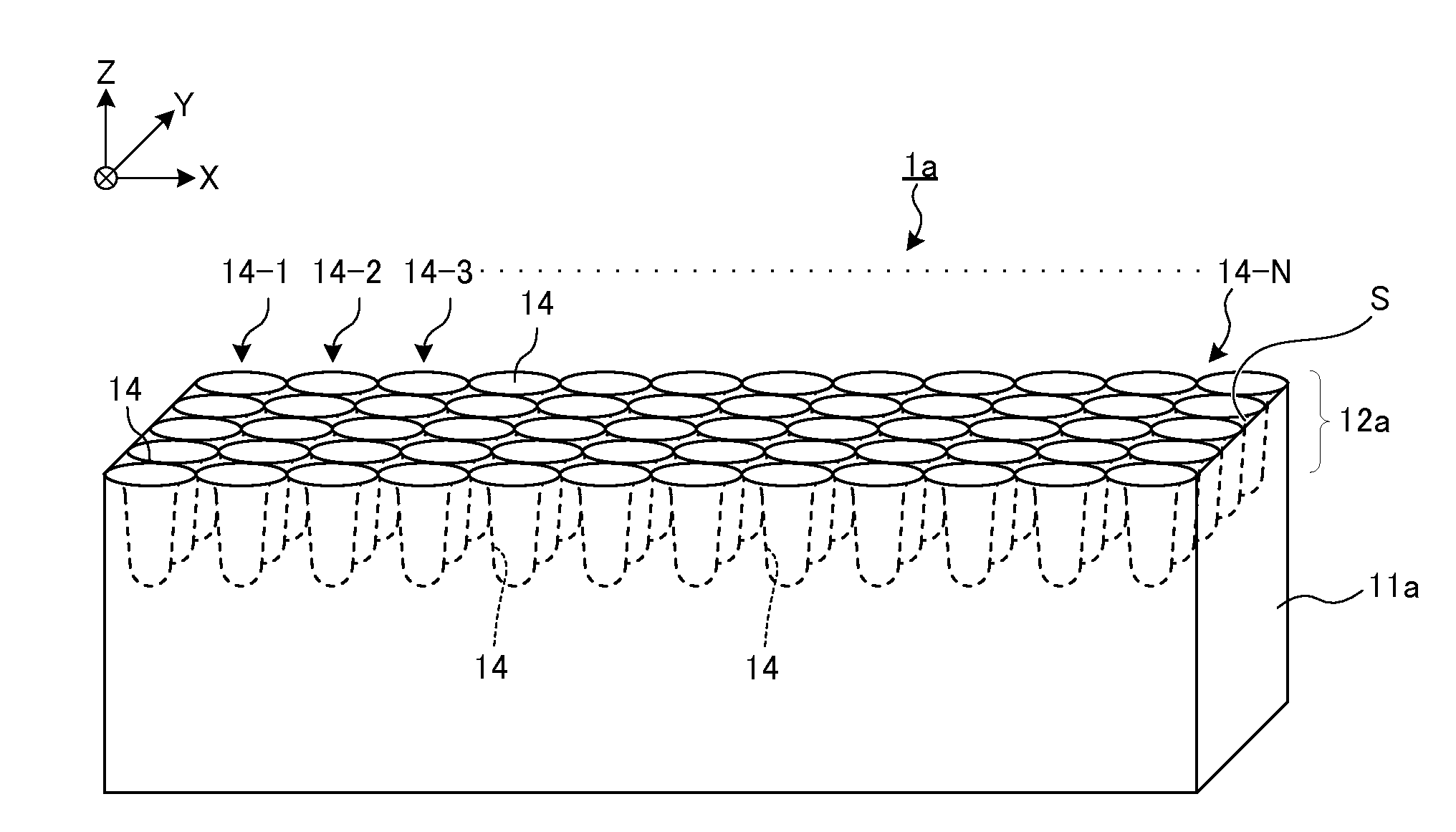
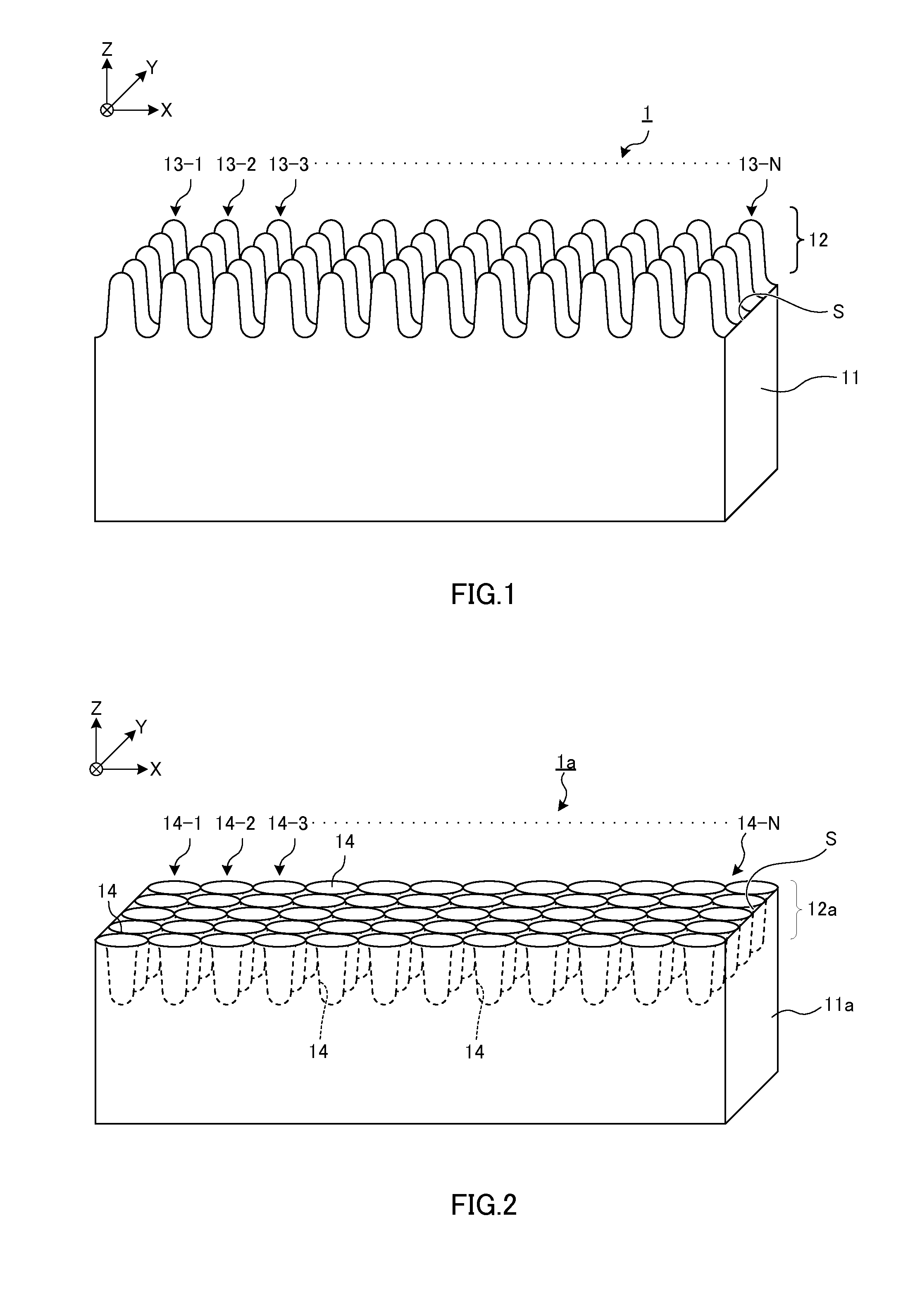
Image

Examples
example 1
Cylindrical Mold Preparation (Preparation of a Mold for Resin Mold Preparation)
[0384]Used as a substrate of a cylindrical mold was a cylindrical quartz glass roll with a diameter of 80 mm and a length of 50 mm. A fine structure (fine concavo-convex structure) was formed on the cylindrical quartz glass roll surface by a direct-write lithography method using a semiconductor laser by the following method.
[0385]First, a resist layer is deposited on the fine structure on the quartz glass surface by a sputtering method. The sputtering method was carried out with power of RF 100 W using CuO (containing 8 atm % of Si) as a target (resist layer). The film thickness of the resist layer after deposition was 20 nm. The cylindrical mold prepared as described above was exposed on the following conditions while rotating at linear speed s=1.0 msec.
[0386]Exposure semiconductor laser wavelength: 405 nm
[0387]Exposure laser power: 3.5 mV
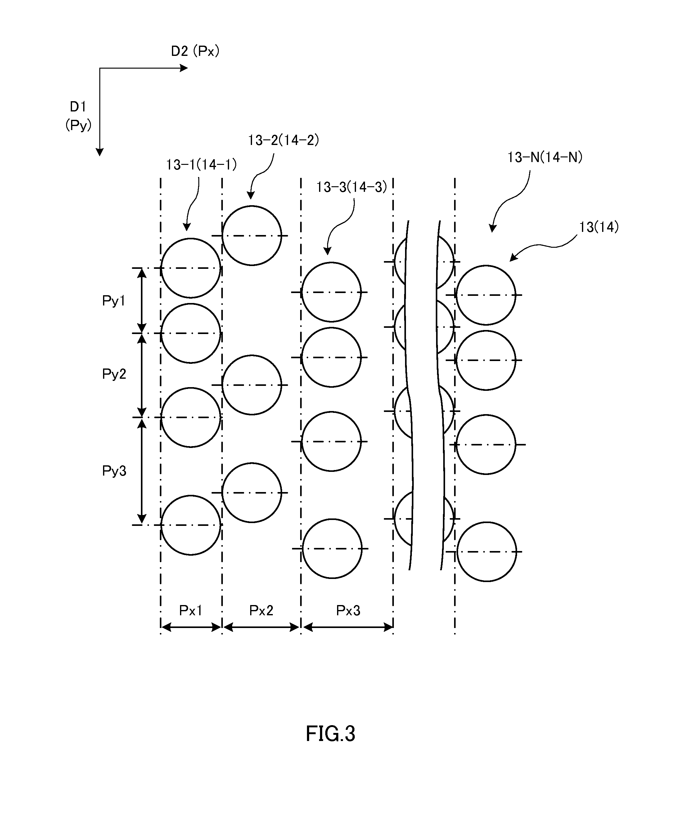
[0388]D2 direction pitch PN: 398 nm[0389]Variable width δ2 with re...
example 2
[0421]A cylindrical mold prepared as in Example 1 was exposed on the following conditions while rotating at linear speed s=1.0 m / sec.
[0422]Exposure semiconductor laser wavelength: 405 nm
[0423]Exposure laser power: 3.5 mV
[0424]D2 direction pitch Px: 606 nm[0425]Variable width δ2 with respect to the D2 direction pitch Px: 61 nm[0426]Long period PxL in the D2 direction of the variable width=2: 6 μm
[0427]D1 direction pitch Py: 700 nm[0428]Variable width δ1 with respect to the D1 direction pitch Py: 70 nm[0429]Long period PyL in the D1 direction of the variable width δ1: 7 μm
[0430]Next, as in Example 1, obtained was a reel-shaped transparent resin mold (length 200 m, width 300 mm) with the fine structure inversely transferred. Using the reel-shaped transparent resin mold, an organic EL device (Example 2) was prepared as in Example 1.
example 3
[0431]A cylindrical mold prepared as in Example 1 was exposed on the following conditions while rotating at linear speed s=1.0 m / sec.
[0432]Exposure semiconductor laser wavelength: 405 nm
[0433]Exposure laser power: 3.5 mV
[0434]D2 direction pitch Px: 700 nm
[0435]D1 direction pitch Py: 700 nm
[0436]Control of the reference signal of the pitch Py was made only initially.
[0437]Next, as in Example 1, obtained was a reel-shaped transparent resin mold (length 200 m, width 300 mm) with the surface structure inversely transferred.
[0438]The surface of the prepared reel-shaped transparent resin mold was observed with the scanning electron microscope. Convex portions were arranged in the shape of lines with the set pitch Py in the D1 direction. Further, the line-shaped convex portions were repeatedly provided with the predetermined pitch Px in the D2 direction. Furthermore, the shift amounts σ were irregular among line-shaped convex portions arranged adjacent to one another in the D2 direction.
[0...
PUM
 Abstract
Description
Claims
Application Information
 - R&D
- Intellectual Property
- Life Sciences
- Materials
- Tech Scout
- Unparalleled Data Quality
- Higher Quality Content
- 60% Fewer Hallucinations
Browse by: Latest US Patents, China's latest patents, Technical Efficacy Thesaurus, Application Domain, Technology Topic, Popular Technical Reports.
© 2025 PatSnap. All rights reserved.Legal|Privacy policy|Modern Slavery Act Transparency Statement|Sitemap|About US| Contact US: help@patsnap.com