Wafer packaging method

a packaging method and wafer technology, applied in the direction of electrical equipment, semiconductor/solid-state device manufacturing, semiconductor devices, etc., can solve the problems of easy cracking of the frame, difficult movement of the wafer, and difficulty in the placement of the wafer on the iron frame, so as to improve the yield rate of the wafer and improve the convenience of the wire bonding process.

Active Publication Date: 2014-08-28
XINTEC INC
View PDF1 Cites 0 Cited by
  • Summary
  • Abstract
  • Description
  • Claims
  • Application Information

AI Technical Summary

Benefits of technology

The present invention provides a method for packaging wafers that includes steps to protect the wafer surface and improve its adhesion to a supporting surface. The method also allows for the removal of a light transmissive carrier and the temporary bonding layer without causing damage to the wafer. Additionally, the method includes steps to improve the image sensing ability of the wafer by eliminating the need for an optical glass sheet. The technical effects of the invention include improved yield rate, prevention of pollution or corrosion, and improved wire bonding process convenience.

Problems solved by technology

However, in that the thickness of the wafer is significantly thin (e.g., around 150 μm), the wafer having ball grid array (BGA) is very difficult for the movement.
If the surface of the wafer has no the optical glass sheet, the wafer, frame in the placement of the wafer on the iron frame, is easily cracked due to warpage, or hardly to precisely place on the tape of the iron.
As a result, after the process of bonding, such as Dam On Glass (DOG), of the optical glass sheet to the wafer the conductive pad of the wafer is contaminated during a subsequent dicing process or a chemical liquid process, so as to reduce the yield rate of the wafer.

Method used


Image

  • Wafer packaging method
  • Wafer packaging method
  • Wafer packaging method

Examples


Embodiment Construction

[0051]Reference will now be made in detail to the present embodiments of the invention, examples of which are illustrated in the accompanying drawings. Wherever possible, the same reference numbers are used in the drawings and the description to refer to the same or like parts.

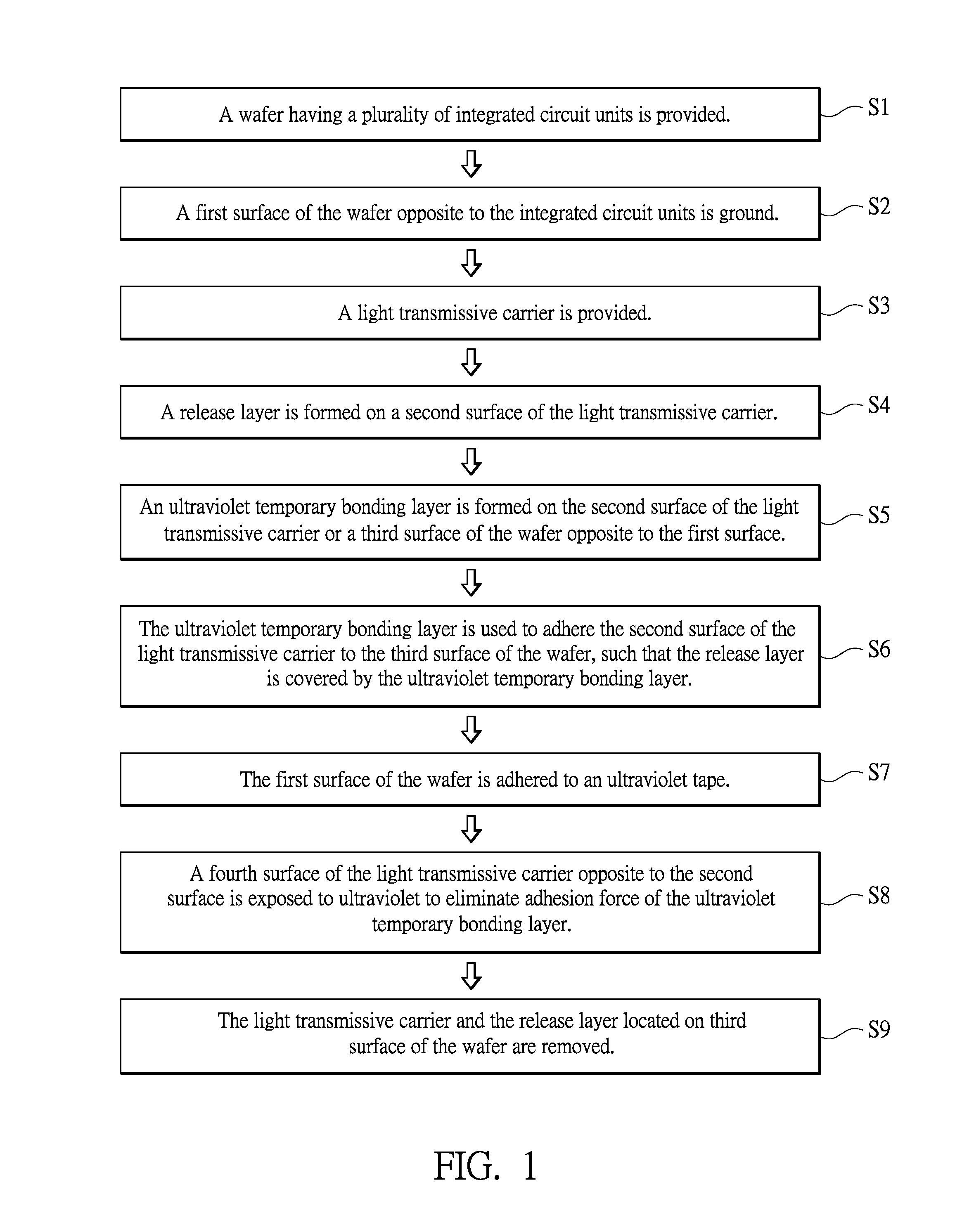
[0052]FIG. 1 is a flow chart of a wafer packaging method according to one embodiment of the present invention. In step S1, a wafer having a plurality of integrated circuit units is provided. Thereafter in step S2, a first surface of the wafer opposite to the integrated circuit units is ground (“ground” is referred to as the verb tense of “grind”). Next in step S3, a light transmissive carrier is provided. Thereafter in step S4, a release layer is formed on a second surface of the light transmissive carrier. Next in step S5, an ultraviolet temporary bonding layer is formed on the second surface of the light transmissive carrier or a third surface of the wafer opposite to the first surface. Thereafter in step S6...


PUM


Abstract

A wafer packaging method includes the following steps. A wafer having a plurality of integrated circuit units is provided. A first surface of the wafer opposite to the integrated circuit units is ground. A release layer is formed on a second surface of a light transmissive carrier. An ultraviolet temporary bonding layer is formed on the second surface of the light transmissive carrier or a third surface of the wafer. The ultraviolet temporary bonding layer is used to adhere the second surface of the light transmissive carrier to the third surface of the wafer. The first surface of the wafer is adhered to an ultraviolet tape. A fourth surface of the light transmissive carrier is exposed to ultraviolet to eliminate adhesion force of the ultraviolet temporary bonding layer. The light transmissive carrier and the release layer are removed.

Description

RELATED APPLICATIONS[0001]This application claims priority to U.S. provisional Application Ser. No. 61 / 770,025, filed Feb. 27, 2013, which is herein incorporated by reference.BACKGROUND[0002]1. Field of Invention[0003]The present invention relates to a wafer packaging method.[0004]2. Description of Related Art[0005]In manufacture of an image sensor chip, e.g., a CMOS chip, on a wafer, an optical glass sheet is often used to cover the surface of the wafer for protection, to avoid dust attaching on the image sensing region of the wafer. However, as a chip diced from the wafer and used in an electrical product, the chip is aligned with a light-transmissive sheet, which is usually disposed on the housing of the electrical product and has the protection ability of the light-transmissive sheet similar with that of the optical glass sheet on the surface of the chip.[0006]In case the surface of the wafer is not covered by the optical glass sheet, the light transmittance of the wafer may be ...

Claims


Application Information

Patent Timeline
Patent Type & Authority Applications(United States)
IPC IPC(8): H01L31/0203H01L21/683
CPCH01L31/0203H01L21/6836H01L21/6835H01L2221/68327H01L2221/6834H01L2221/68381H01L27/14618H01L27/14683H01L2224/48091H01L2924/16235H01L2924/00014
Inventor CHANG, YI-MINGLIU, KUO-HUAWANG, YI-CHENGCHANG, SHENG-YEN
Owner XINTEC INC
Why Eureka
Try Eureka