Semiconductor device and method for manufacturing semiconductor device
- Summary
- Abstract
- Description
- Claims
- Application Information
AI Technical Summary
Benefits of technology
Problems solved by technology
Method used
Image


Examples
first exemplary embodiment
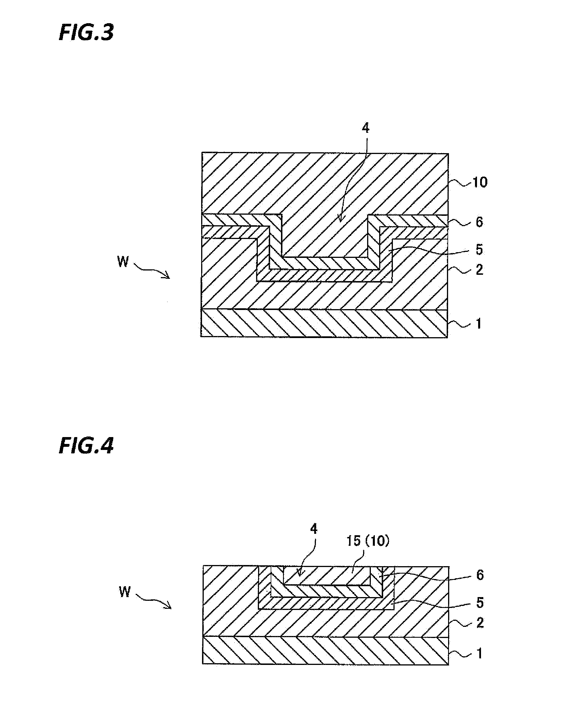
[0032]First, a manufacturing process of manufacturing a Cu wiring structure according to a first exemplary embodiment of the present disclosure will be described. FIGS. 1 to 5 are cross-sectional views of a substrate for describing a manufacturing process of manufacturing a Cu wiring structure according to the present exemplary embodiment. That is, FIGS. 1 to 5 illustrate a process of forming a Cu wiring on a top surface of a substrate main body 1 in a substrate W made of, for example, Si.
[0033]First, as illustrated in FIG. 1, an interlayer insulating film 2 which is a CF film (fluorine-added carbon film) is formed on the substrate main body 1 by a deposition method using plasma generated by, for example, a radial line slot antenna. Subsequently, a wiring groove 4 is formed on the surface of the interlayer insulating film 2 by photolithography and reactive ion etching (RIE).
[0034]Then, as illustrated in FIG. 2, a fluorine barrier film 5 and a barrier metal (“BM”) film 6 are successi...
second exemplary embodiment
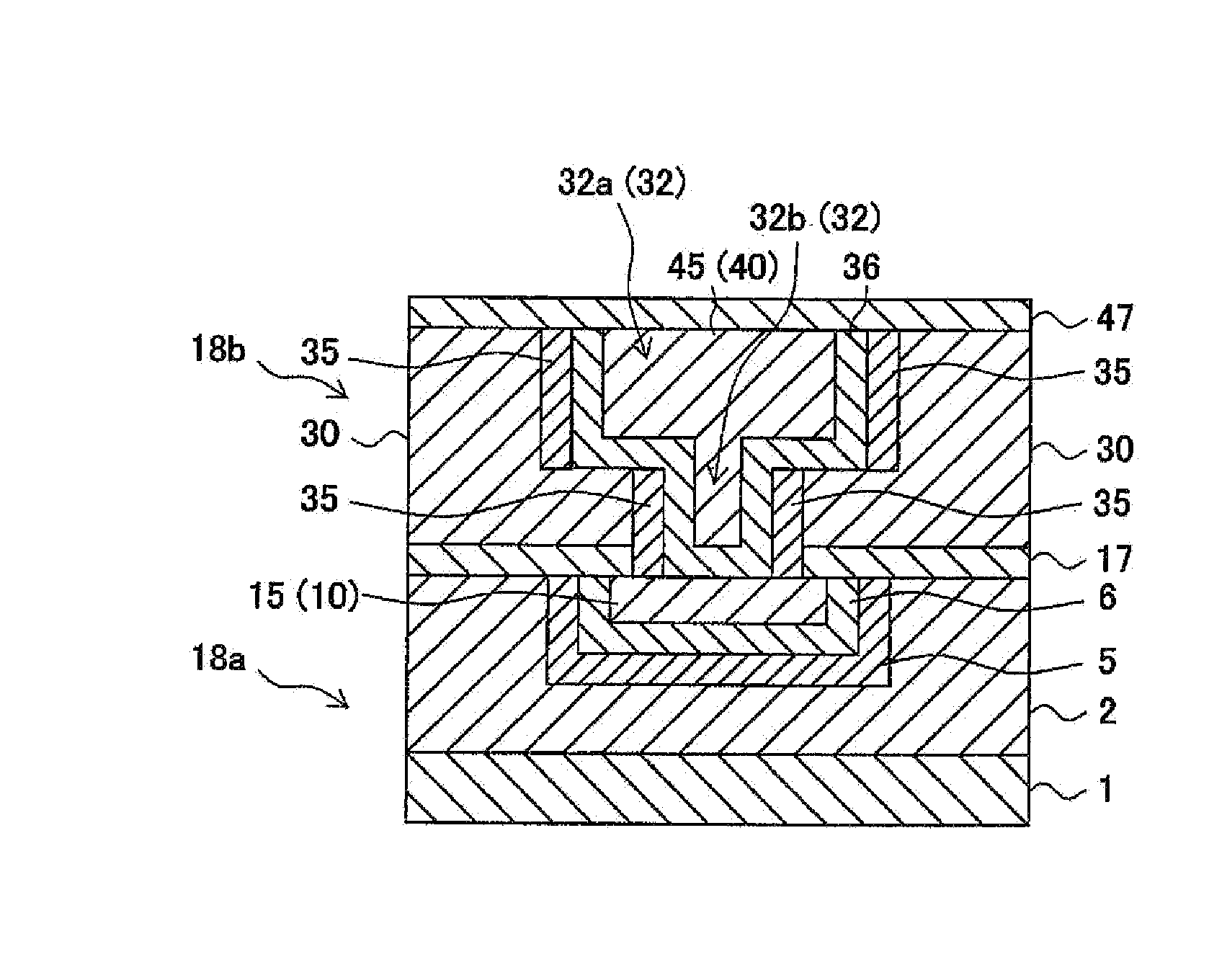
[0045]Therefore, descriptions will be made on a so-called double damascene wiring structure according to the second exemplary embodiment of the present disclosure, in which two Cu wiring structures are connected to each other through a via wiring to be formed in two overlapping layers.
[0046]FIGS. 6 to 13 are cross-sectional views of a substrate for describing a process of manufacturing a Cu wiring structure according to the present exemplary embodiment, in which Cu wiring structures 18a (a first layer) and 18b (a second layer) disposed in two layers are via-connected. In the second exemplary embodiment, descriptions will be made on a case where the Cu wiring structure 18 (that is, 18a herein) manufactured as described in the first exemplary embodiment is a first layer, and the Cu wiring structure 18b as a second layer is formed above the first layer as illustrated in the drawings.
[0047]First, as illustrated in FIG. 6, an interlayer insulating film 30 which is a CF film is formed by ...
examples
[0058]It has been found that when a CF film is used as an interlayer insulating film in a manufacturing process of a conventional Cu wiring structure, a barrier metal layer may suffer from reduction of a barrier property that suppresses Cu from being diffused and a leakage current may be increased in the Cu wiring structure. This finding will be described in detail in Examples to be described below.
[0059]First, the inventors performed an evaluation on a change of a leakage current while performing an annealing process in a case where a CF film was used as an interlayer insulating film, and in a case where BD (Black Diamond) was used as an interlayer insulating film. FIG. 14 is a graph illustrating a change of a leakage current (at a voltage load of 20V) when the annealing process was performed under a condition of 350° C. in which the change of the leakage current was measured on a semiconductor device manufactured by using a CF film (“Std” in the graph) as an interlayer insulating ...
PUM
 Abstract
Description
Claims
Application Information
 - R&D
- Intellectual Property
- Life Sciences
- Materials
- Tech Scout
- Unparalleled Data Quality
- Higher Quality Content
- 60% Fewer Hallucinations
Browse by: Latest US Patents, China's latest patents, Technical Efficacy Thesaurus, Application Domain, Technology Topic, Popular Technical Reports.
© 2025 PatSnap. All rights reserved.Legal|Privacy policy|Modern Slavery Act Transparency Statement|Sitemap|About US| Contact US: help@patsnap.com