Radiation-Emitting Semiconductor Component

Active Publication Date: 2014-08-07
OSRAM OLED
View PDF6 Cites 6 Cited by
  • Summary
  • Abstract
  • Description
  • Claims
  • Application Information

AI Technical Summary

Benefits of technology

The invention is a semiconductor component that can improve image quality while also producing high optical output powers.

Problems solved by technology

This can lead to a reduced imaging quality, for example, in projection applications on account of so-called speckle.
This problem makes it more difficult in particular to realize large-area projection devices of high light intensity using laser diodes as radiation source.

Method used


Image

  • Radiation-Emitting Semiconductor Component
  • Radiation-Emitting Semiconductor Component
  • Radiation-Emitting Semiconductor Component

Examples


Embodiment Construction

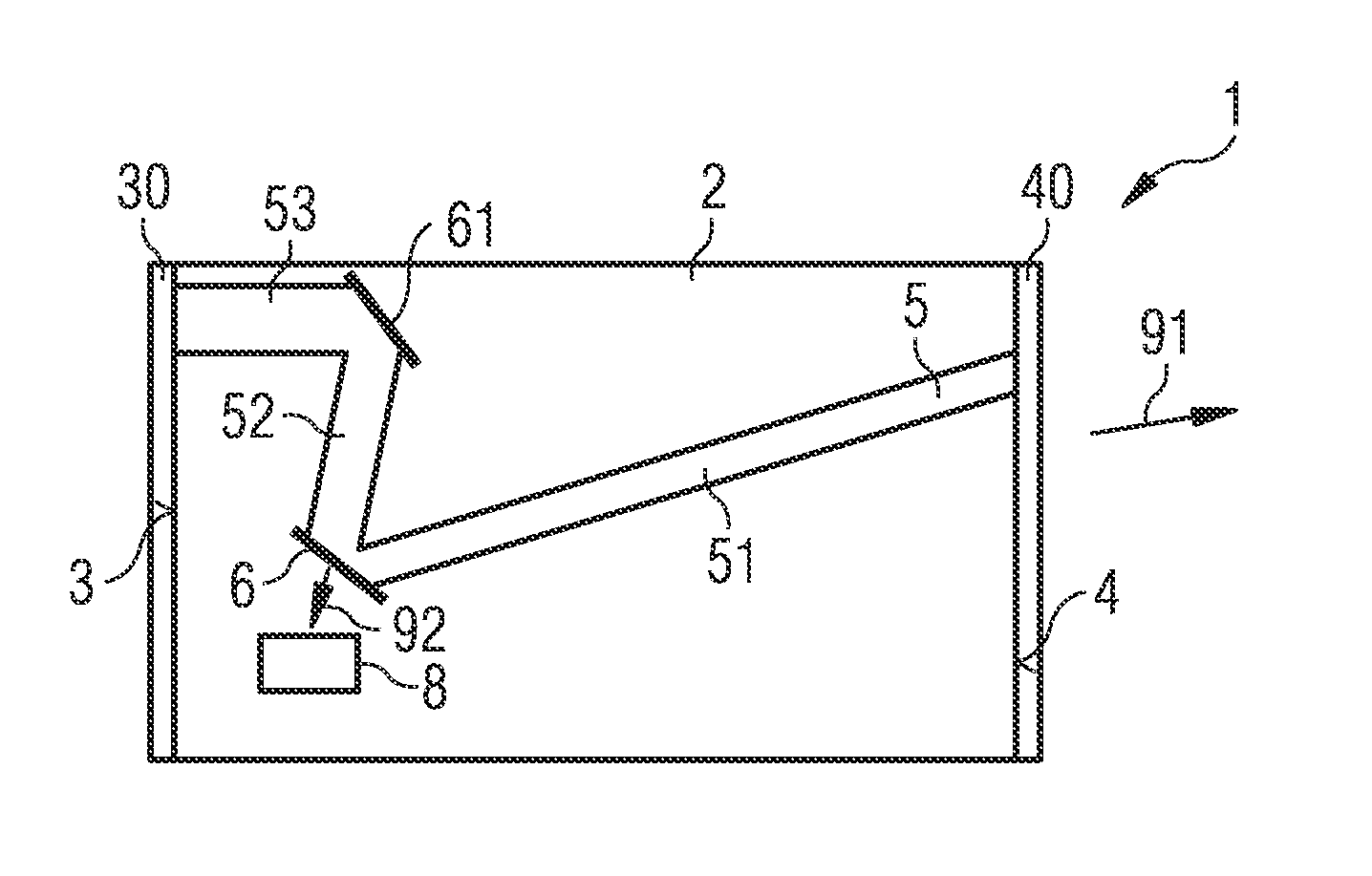
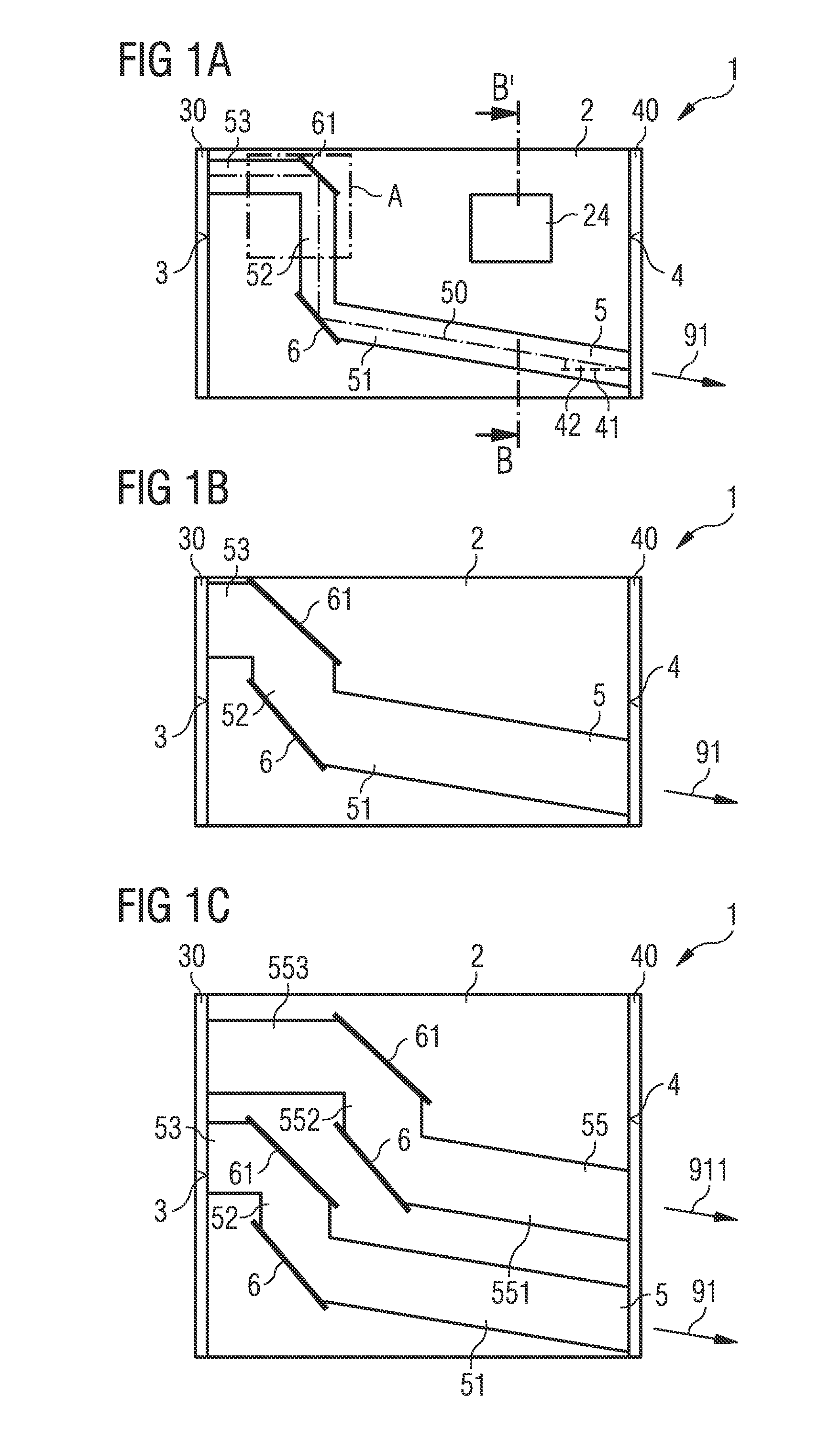
[0045]FIGS. 1A to 1C in each case illustrate an exemplary embodiment of a semiconductor component 1 in schematic plan view. The semiconductor component has a semiconductor body 2, in which a waveguide 5 is formed. The waveguide 5 is provided for guiding a radiation generated in an active region of the semiconductor body 2 in a lateral direction, that is to say in a direction running along a main extension plane of the semiconductor layer sequence of the semiconductor body.

[0046]An exemplary embodiment of a suitable layer sequence for the semiconductor body 2 is described in greater detail in connection with FIG. 9.

[0047]In a lateral direction, the semiconductor body 2 with the waveguide 5 extends between a mirror surface 3 and a coupling-out surface 4. In the exemplary embodiment shown, the mirror surface and the coupling-out surface are formed at opposite sides of the semiconductor body 2 and furthermore run parallel to one another.

[0048]The mirror surface 3 is provided with a high...


PUM


Abstract

A radiation-emitting semiconductor component includes a semiconductor body. The semiconductor body has a semiconductor layer sequence having an active region provided for generating radiation. The semiconductor component has a waveguide, which is provided for laterally guiding the radiation generated in the active region and which extends between a mirror surface and a coupling-out surface. The waveguide meets the mirror surface perpendicularly and forms an acute angle with a normal to the coupling-out surface.

Description

[0001]This patent application is a national phase filing under section 371 of PCT / EP2012 / 064894, filed Jul. 30, 2012, which claims the priority of German patent application 10 2011 111 604.8, filed Aug. 25, 2011, each of which is incorporated herein by reference in its entirety.TECHNICAL FIELD[0002]The present application relates to a radiation-emitting semiconductor component comprising a semiconductor body.[0003]Laser sources, for example, semiconductor lasers with ridge waveguide geometry (ridge waveguide laser), can have a very narrowband emission spectrum. This can lead to a reduced imaging quality, for example, in projection applications on account of so-called speckle. This problem makes it more difficult in particular to realize large-area projection devices of high light intensity using laser diodes as radiation source.SUMMARY OF THE INVENTION[0004]Embodiments of the invention provide a semiconductor component with which the imaging quality can be improved and at the same t...

Claims


Application Information

Patent Timeline
IPC IPC(8): G02B6/125
CPCG02B6/125H01L33/0045H01S5/0264H01S5/1017H01S5/1085H01S2301/166
Inventor KOPP, FABIANLELL, ALFREDEICHLER, CHRISTOPHVIERHEILIG, CLEMENSTAUTZ, SONKE
Owner OSRAM OLED
Why Eureka
Try Eureka