
Piezoelectric bulk wave device, and method of manufacturing the piezoelectric bulk wave device

Active Publication Date: 2014-06-19
MURATA MFG CO LTD
View PDF5 Cites 8 Cited by
  • Summary
  • Abstract
  • Description
  • Claims
  • Application Information

AI Technical Summary

Benefits of technology

This patent text describes a method for producing a piezoelectric thin plate with uniform thickness over the entire substrate surface. By using ion implantation, the position of the high concentration ion-engineered portion becomes uniform over the entire substrate surface, leading to smaller variations in depth. This makes it easier to obtain a piezoelectric thin plate with accurate thickness. Additionally, this method reduces the possibility of defects occurring during the separation of the piezoelectric thin plate due to thermal stress.

Problems solved by technology

However, in a case where thickness shear vibration mode is utilized by using a piezoelectric thin film made of LiTaO3, it is difficult to make the electromechanical coupling coefficient k2 of the thickness shear mode sufficiently high.
For this reason, it is difficult to achieve a wider frequency band or increase the adjustable range of band width.

Method used


Image

  • Piezoelectric bulk wave device, and method of manufacturing the piezoelectric bulk wave device
  • Piezoelectric bulk wave device, and method of manufacturing the piezoelectric bulk wave device
  • Piezoelectric bulk wave device, and method of manufacturing the piezoelectric bulk wave device

Examples


Embodiment Construction

[0032]Hereinafter, the present invention will be explained by way of specific embodiments of the present invention with reference to the drawings.

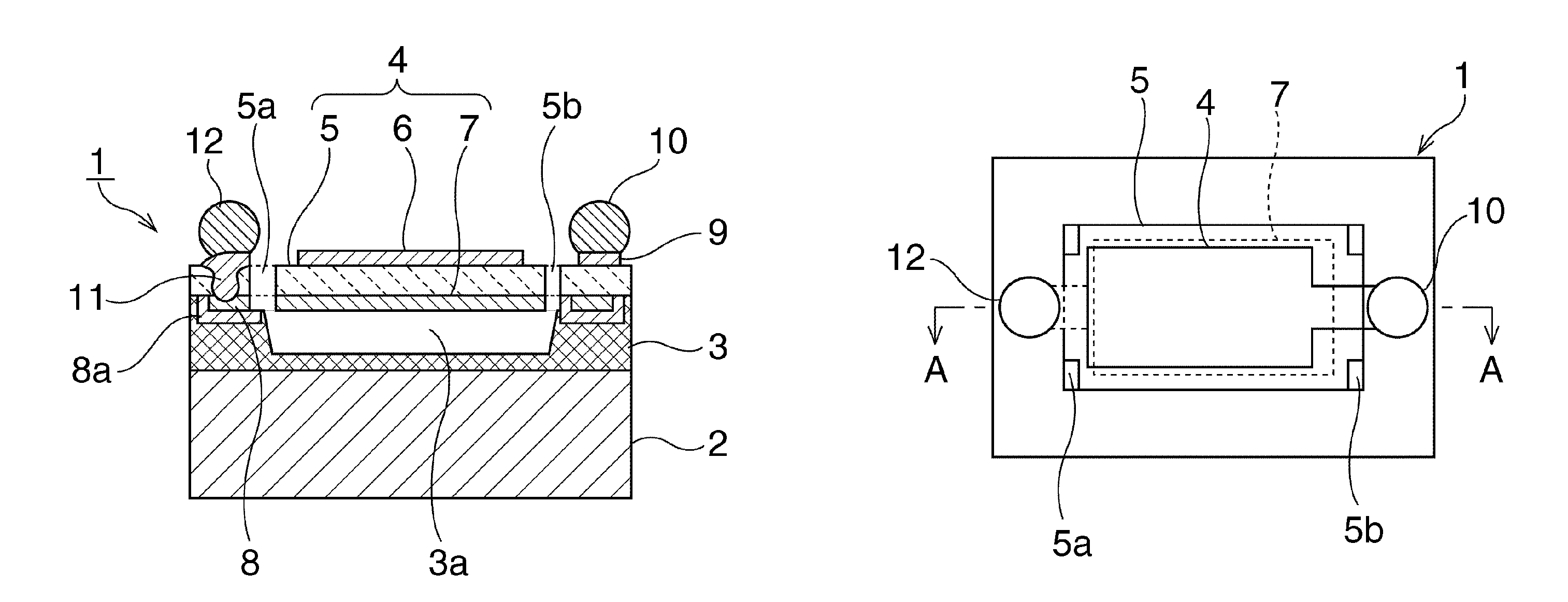
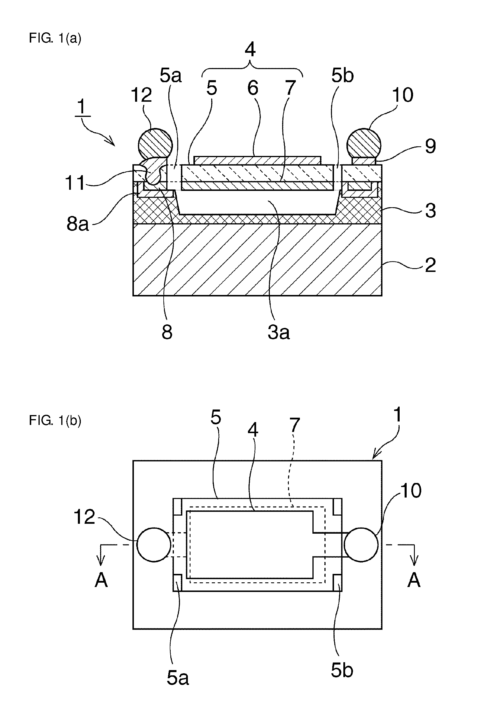
[0033]FIGS. 1(a) and 1(b) are a schematic elevational cross-sectional view and a plan view, respectively, of a piezoelectric bulk wave device according to an embodiment of the present invention.

[0034]A piezoelectric bulk wave device 1 according to this embodiment has a support substrate 2. The support substrate 2 is formed by a suitable insulating body or piezoelectric body. In this embodiment, the support substrate 2 is formed by alumina.

[0035]An insulating layer 3 is formed on the support substrate 2. While the insulating layer 3 is made of silicon oxide in this embodiment, the insulating layer3 may be made of a suitable insulating material such as LiTaO3, LiNbO3, sapphire, or glass. Alumina, glass, and LiNbO3 are preferred because these materials are inexpensive in comparison to LiTaO3 and sapphire, and easy to manufacture. A recess 3a ...


PUM

PropertyMeasurementUnit
Thicknessaaaaaaaaaa
Angleaaaaaaaaaa
Angleaaaaaaaaaa

Abstract

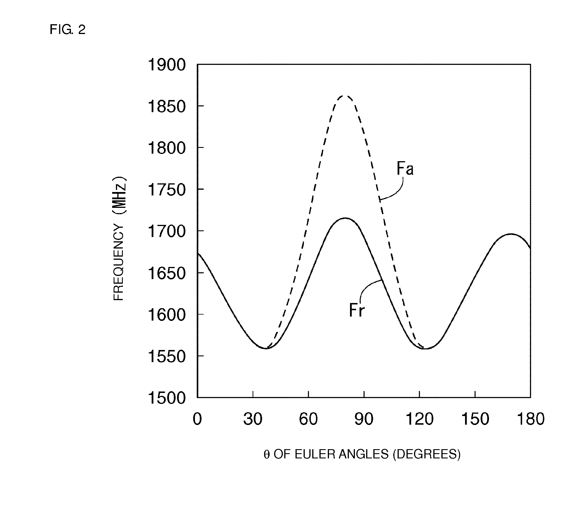
A piezoelectric bulk wave device that includes a piezoelectric thin plate that is made of LiTaO3, and first and second electrodes that are provided in contact with the piezoelectric thin plate. The piezoelectric bulk wave device utilizes the thickness shear mode of the piezoelectric thin plate made of LiTaO3, and of the Euler Angles (φ, θ, φ) of LiTaO3, φ is 0°, and θ is in the range of not less than 54° and not more than 107°.

Description

CROSS REFERENCE TO RELATED APPLICATIONS[0001]The present application is a continuation of International application No. PCT / JP2012 / 071639, filed Aug. 28, 2012, which claims priority to Japanese Patent Application No. 2011-190344, filed Sep. 1, 2011, the entire contents of each of which are incorporated herein by reference.FIELD OF THE INVENTION[0002]The present invention relates to a piezoelectric bulk wave device using LiTaO3, and a method of manufacturing the piezoelectric bulk wave device. More specifically, the present invention relates to a piezoelectric bulk wave device that utilizes a bulk wave of thickness shear mode as a bulk wave, and a method of manufacturing the piezoelectric bulk wave device.BACKGROUND OF THE INVENTION[0003]In related art, piezoelectric thin film devices are used for oscillators, filters, and the like. For example, a piezoelectric thin film device illustrated in FIG. 16 is disclosed in Patent Document 1 mentioned below. A piezoelectric thin film device ...

Claims


Application Information

Patent Timeline
IPC IPC(8): H01L41/18H01L41/29
CPCH03H3/02H03H9/02015H03H9/0595H03H9/173Y10T29/42H10N30/85H10N30/852H10N30/06
Inventor KANDO, HAJIME
Owner MURATA MFG CO LTD
Learn More