
High-density stacked planar metal-insulator-metal capacitor structure and method for manufacturing same

a technology of metal-insulator and capacitor, which is applied in the direction of capacitor, semiconductor device details, semiconductor/solid-state device devices, etc., can solve the problems of significant power supply voltage droop at the integrated circuit die and performance degradation, and achieve the effect of reducing the magnitude of power supply voltage droop, reducing system performance degradation, and high on-chip capacitance density

Inactive Publication Date: 2014-06-12
ADVANCED MICRO DEVICES INC
View PDF14 Cites 53 Cited by
  • Summary
  • Abstract
  • Description
  • Claims
  • Application Information

AI Technical Summary

Benefits of technology

The patent aims to address the issue of power supply voltage droops in computer systems. By increasing the on-chip capacitance density, the patent aims to reduce the magnitude of these droops, which can degrade system performance and introduce design complexity. The goal is to provide higher capacitance without adding substantial process complexity or cost.

Problems solved by technology

An abrupt change in current flowing through such inductive package interconnects, due to a rapid change in circuit activity on the die, will cause a significant power supply voltage droop at the integrated circuit die.
These power supply voltage droops cause performance degradation, and impose design complexity and conservative performance margining to prevent timing failures when circuit delays suddenly increase during such droops.

Method used


Image

  • High-density stacked planar metal-insulator-metal capacitor structure and method for manufacturing same
  • High-density stacked planar metal-insulator-metal capacitor structure and method for manufacturing same
  • High-density stacked planar metal-insulator-metal capacitor structure and method for manufacturing same

Examples


Embodiment Construction

[0006]Accordingly, it would be desirable to provide higher on-chip capacitance density, to therefore reduce the magnitude of power supply voltage droops. This would mitigate system performance degradation and circumvent some amount of design complexity. It would be further desirable to provide such higher on-chip capacitance density without a substantial increase in process complexity or cost.

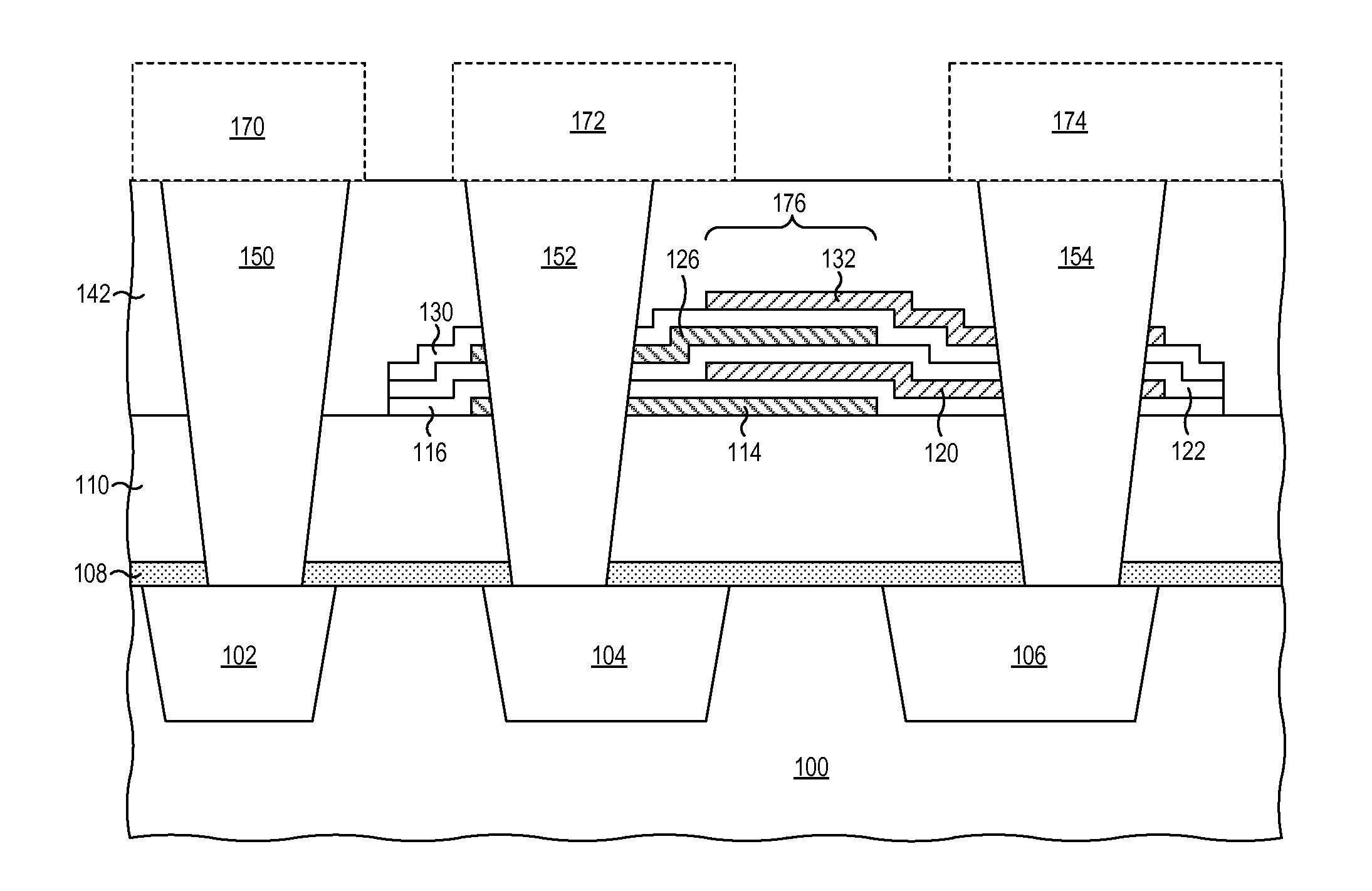
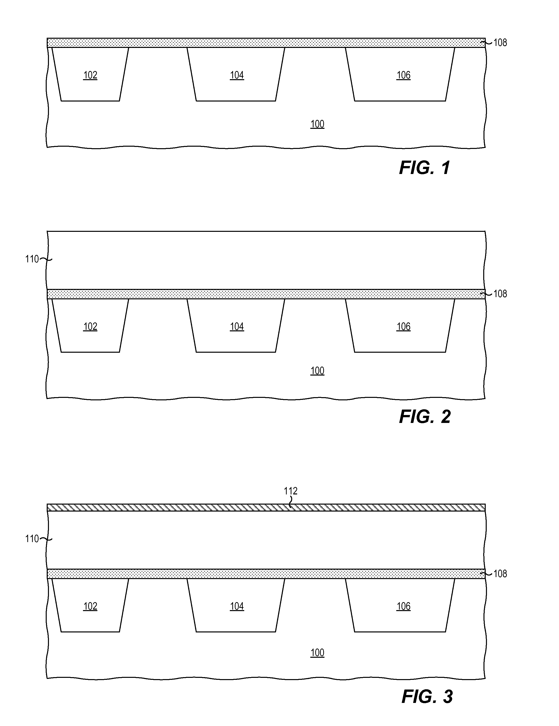
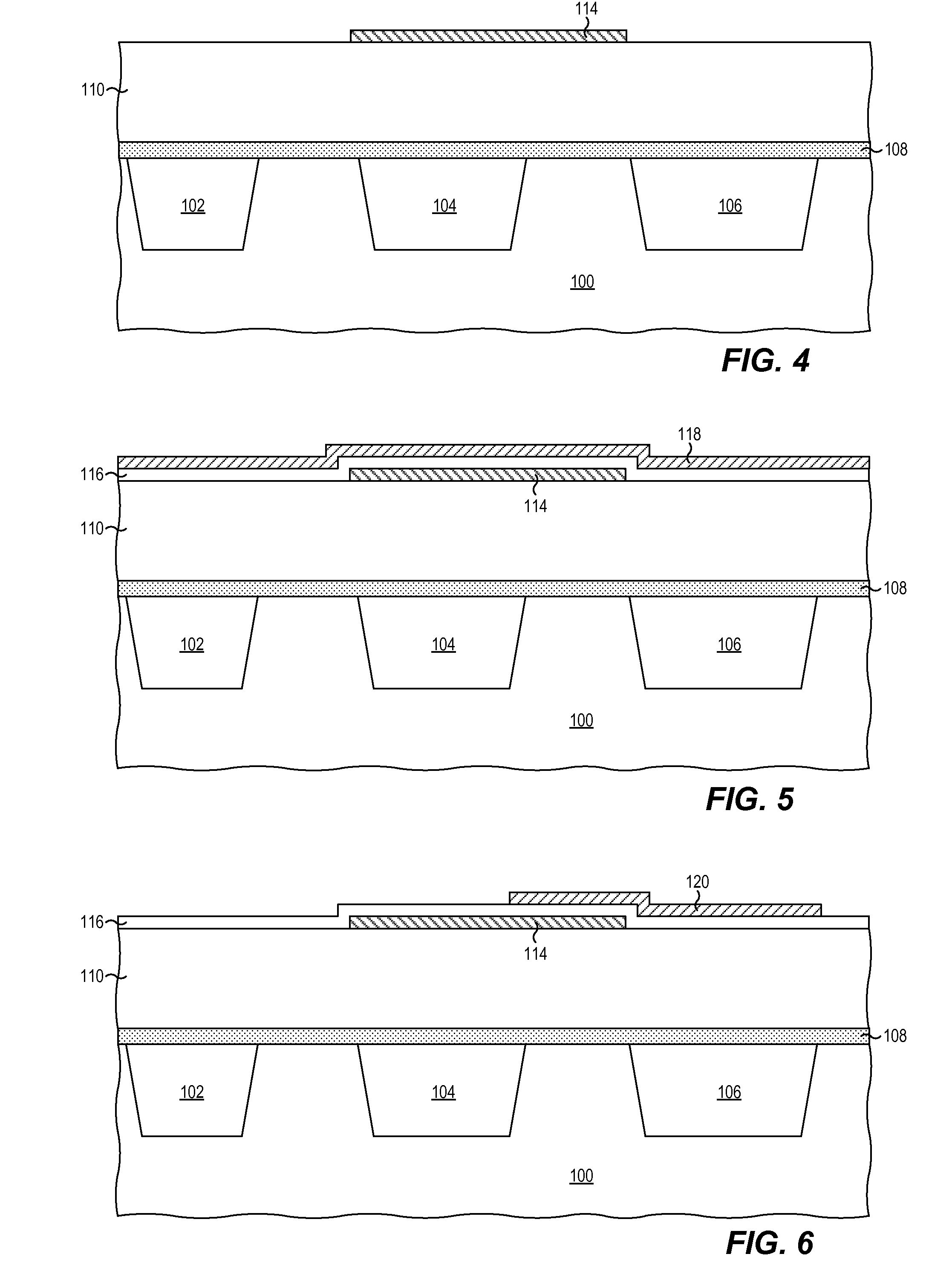
[0007]In one example embodiment, a high-density, stacked, planar metal-insulator-metal (MIM) capacitor structure includes a stack of planar electrodes and interposing dielectric layers. Vertically-alternating electrodes are horizontally-staggered, and vias are formed through the multiple electrodes, so that electrical connection is made circumferentially through the via sidewalls to multiple electrodes through which a given via passes. A MIM capacitor incorporating a multiple-level capacitor stack may be fabricated by repeated usage of the same mask operation for each incremental capacitor stac...


PUM


Abstract

An embodiment of a high-density, stacked, planar metal-insulator-metal (MIM) capacitor structure includes a stack of planar electrodes and interposing dielectric layers. Vertically-alternating electrodes are horizontally-staggered, and vias are formed through the multiple electrodes, so that electrical connection is made circumferentially through the via sidewalls to multiple electrodes through which a given via passes. An MIM capacitor incorporating a multiple-level capacitor stack may be fabricated by repeated usage of the same mask operation for each incremental capacitor stack level, and without requiring additional masks beyond those utilized for the first such level.

Description

CROSS-REFERENCE TO RELATED APPLICATION[0001]This application claims the benefit under 35 U.S.C. §119(e) of U.S. Provisional Application No. 61 / 735,004, filed Dec. 8, 2012, entitled “High-Density Stacked Planar Metal-Insulator-Metal Capacitor Structure and Method for Manufacturing Same” by Alvin Leng Sun Loke and Tin Tin Wee, which application is hereby incorporated by reference in its entirety.BACKGROUND[0002]1. Technical Field[0003]This application relates to metal-insulator-metal capacitor structures, and more particularly relates to monolithic planar metal-insulator-metal capacitor structures.[0004]2. Description of the Related Art[0005]Integrated circuit packaging delivers power to an integrated circuit die through package interconnects that are instrinsically inductive. An abrupt change in current flowing through such inductive package interconnects, due to a rapid change in circuit activity on the die, will cause a significant power supply voltage droop at the integrated circu...

Claims


Application Information

Patent Timeline
IPC IPC(8): H01L49/02
CPCH01L23/5223H01L23/5226H01L28/60H01L2924/0002H01L2924/00
Inventor LOKE, ALVIN LENG SUNWEE, TIN TIN
Owner ADVANCED MICRO DEVICES INC
Learn More