
Scanning electron microscope and scanning transmission electron microscope

a scanning electron microscope and electron microscope technology, applied in material analysis using wave/particle radiation, instruments, nuclear engineering, etc., can solve the problems of not easy to identify the position of atoms, unwanted signals are occasionally observed, and the direction position cannot be identified, so as to achieve the effect of easy visualization

Active Publication Date: 2014-05-22
HITACHI HIGH-TECH CORP
View PDF9 Cites 30 Cited by
  • Summary
  • Abstract
  • Description
  • Claims
  • Application Information

AI Technical Summary

Benefits of technology

The charged particle instrument described in this patent has several advantages. First, it uses secondary electrons to identify atoms, allowing for the observation of atomic size three-dimensional structures. Second, it can easily visualize the structure inside a specimen when the specimen is observed in a superposed manner. Lastly, it can identify differences in elements of surface atoms or material of an object at an atomic size.

Problems solved by technology

In the image of atomic resolution by transmission electrons, it is not easy to identify the position of atoms because the contrast formed by the electron beam focused on the specimen is varied.
As a result, there has been the problem that unwanted signals are occasionally observed.
As a result, the depth direction position cannot be identified, and the field of view is difficult to find.
Further, in the image formed by forward scattered or transmission electrons, the image information is two-dimensional and planar, which is not suitable for stereoscopic structure observation in an atomic size.
Thus, secondary electrons are produced from the wide area, resulting in a decrease in image resolution.
Accordingly, while the image resolution of the secondary electron image is due to the composition of the two events of electron beam probe size and electron diffusion in specimen, atomic resolution has not been achieved in conventional secondary electron images.

Method used


Image

  • Scanning electron microscope and scanning transmission electron microscope
  • Scanning electron microscope and scanning transmission electron microscope
  • Scanning electron microscope and scanning transmission electron microscope

Examples


example 1

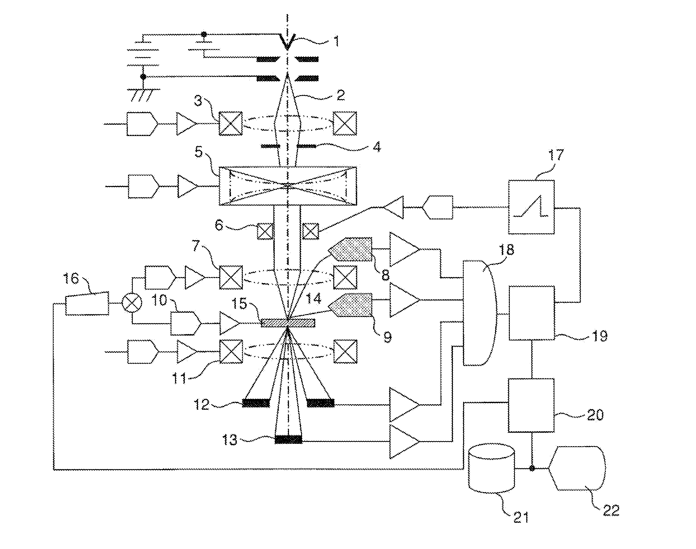
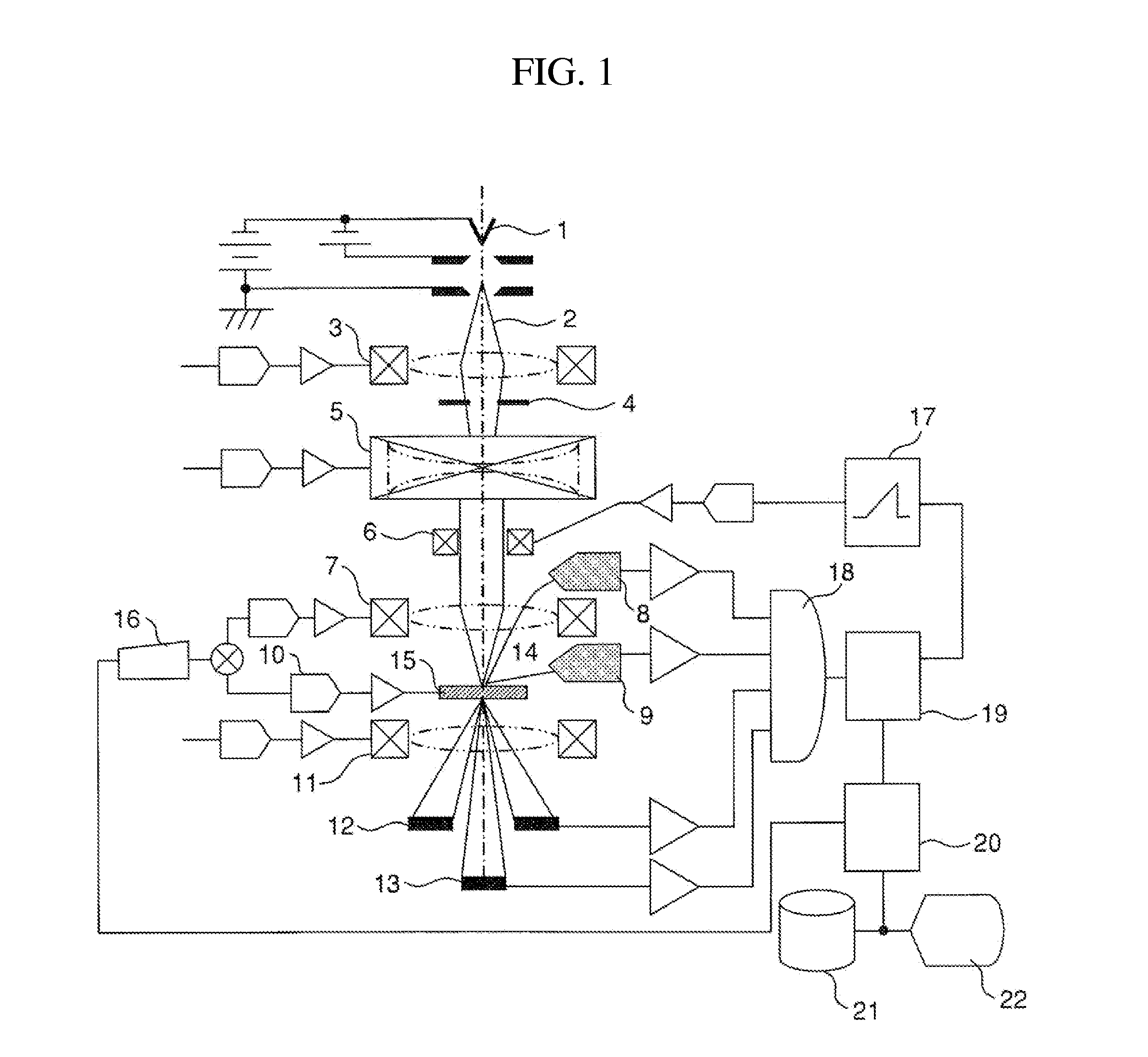
[0056]FIG. 1 is a schematic diagram illustrating an example of a charged particle according to the present invention.

[0057]A primary electron beam 2 generated by an electron gun 1 is condensed by a condenser lens 3 and passed through an aperture 4. While, in FIG. 1, the condenser lens is shown to have one stage for simplicity's sake, the condenser lens may have two stages for changing the illumination angle, or three or more stages for changing the illumination angle while the demagnification of an electron source produced by the electron gun is fixed. The aperture 4 may be set to an arbitrary aperture diameter for obtaining a desired illumination angle on the specimen surface. The illumination angle of the electron beam with which the specimen is irradiated is determined by the aperture diameter. While the aperture is positioned in a subsequent stage to the condenser lens, the installed position is not particularly limited for the purpose of changing the illumination angle.

[0058]In...

example 2

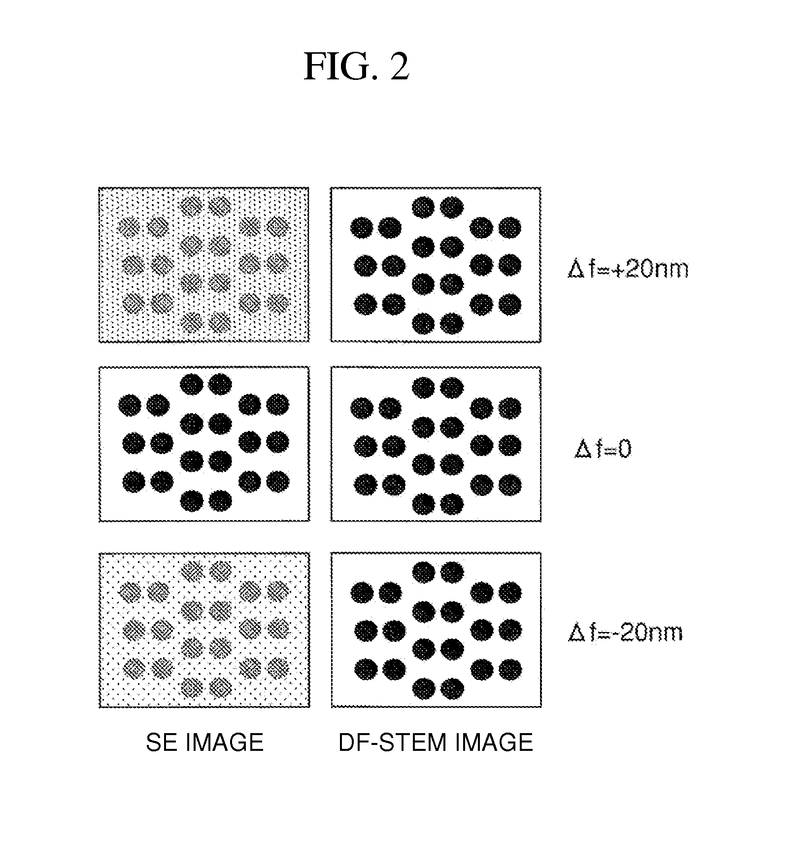
[0068]Next, an example of obtaining a two-dimensional electron image by varying the focal depth will be described.

[0069]First, the relationship between the illumination angle and focal depth of the primary electron beam probe will be described with reference to FIG. 3. The focal depth ZDOF of the electron beam probe size d at the illumination angle α is expressed by expression 2.

[Expression2]ZDOF=dαExpression2

[0070]Thus, when the electron beam probe size d is fixed, the focal depth becomes shallower as the illumination angle of the electron beam is increased. Accordingly, in order to double the focal depth, the electron beam illumination angle may be halved.

[0071]FIG. 4 is a diagram illustrating the relationship between the incident electron beam on the specimen and a secondary electron image of the specimen, which has structures in the depth direction of the incident electron beam. For example, a structure A has an elemental composition in the specimen surface layer portion differe...

example 3

[0078]FIG. 5 is a diagram illustrating the relationship between a specimen having a tapered structure and the electron beam incident thereon. By using the specimen with the tapered structure, the magnitude of focal depth and the amount of defocus can be measured. The specimen is fabricated and prepared by designing the size of the structure such that, for example, the length of the specimen uppermost surface is Ltop, the length of the specimen lowermost surface is Lbottom, and the taper angle is θ. The specimen with the tapered structure may be fabricated through epitaxial growth of different materials on a single crystal wafer by a manufacturing technique such as sputtering (physical vapor deposition), chemical vapor deposition (CVD), or molecular beam epitaxy (MBE), followed by selective etching of specific areas.

[0079]The focal depth measurement is performed as follows. Under the condition that the focal depth at the illumination angle α is ZDOF, a secondary electron image is gen...


PUM


Abstract

A scanning transmission electron microscope according to the present invention includes an electron lens system having a small spherical aberration coefficient for enabling three-dimensional observation of a 0.1 nm atomic size structure. The scanning transmission electron microscope according to the present invention also includes an aperture capable of changing an illumination angle; an illumination electron lens system capable of changing the probe size of an electron beam probe and the illumination angle; a secondary electron detector (9); a transmission electron detector (13); a forward scattered electron beam detector (12); a focusing unit (16); an image processor for identifying image contrast; an image processor for computing image sharpness; a processor for three-dimensional reconstruction of an image; and a mixer (18) for mixing a secondary electron signal and a specimen forward scattered electron signal.

Description

TECHNICAL FIELD[0001]The present invention relates to a scanning transmission electron microscope, particularly to a charged particle instrument for forming a three-dimensional image based on a specimen secondary electron scanning image having an atomic resolution and a specimen transmitted electron image, a scanning transmission electron microscope for visualizing an internal structure of a specimen when the observed specimen has different internal structures or compositions, and a scanning transmission electron microscope for element identification based on a combination of a specimen secondary electron scanning image and a scanned specimen magnified image by forward scattered electrons.BACKGROUND ART[0002]In a scanning electron microscope or a scanning transmission electron microscope that scans a specimen with an electron beam to obtain a magnified image of the specimen, various kinds of electrons are obtained due to the interaction between the specimen and the irradiation prima...

Claims


Application Information

Patent Timeline
Patent Type & Authority Applications(United States)
IPC IPC(8): H01J37/26H01J37/28
CPCH01J37/28H01J37/263H01J37/244H01J2237/0455H01J2237/153H01J2237/225H01J2237/24475H01J2237/2448H01J2237/2611G01N23/2206H01J37/153H01J2237/2802H01J2237/226H01J37/21H01J2237/21H01J2237/0492H01J2237/221H01J2237/1532
Inventor INADA, HIROMINAKAMURA, KUNIYASU
Owner HITACHI HIGH-TECH CORP
Learn More