Read-disturbance-free nonvolatile content addressable memory (CAM)
a nonvolatile, addressable memory technology, applied in the field of read-disturbance-free content addressable memory (cam), can solve the problems of low power, high density, and low power density of meram, and achieve the effect of high performance read-disturbance-free operation
- Summary
- Abstract
- Description
- Claims
- Application Information
AI Technical Summary
Benefits of technology
Problems solved by technology
Method used
Image
Examples
embodiment 10
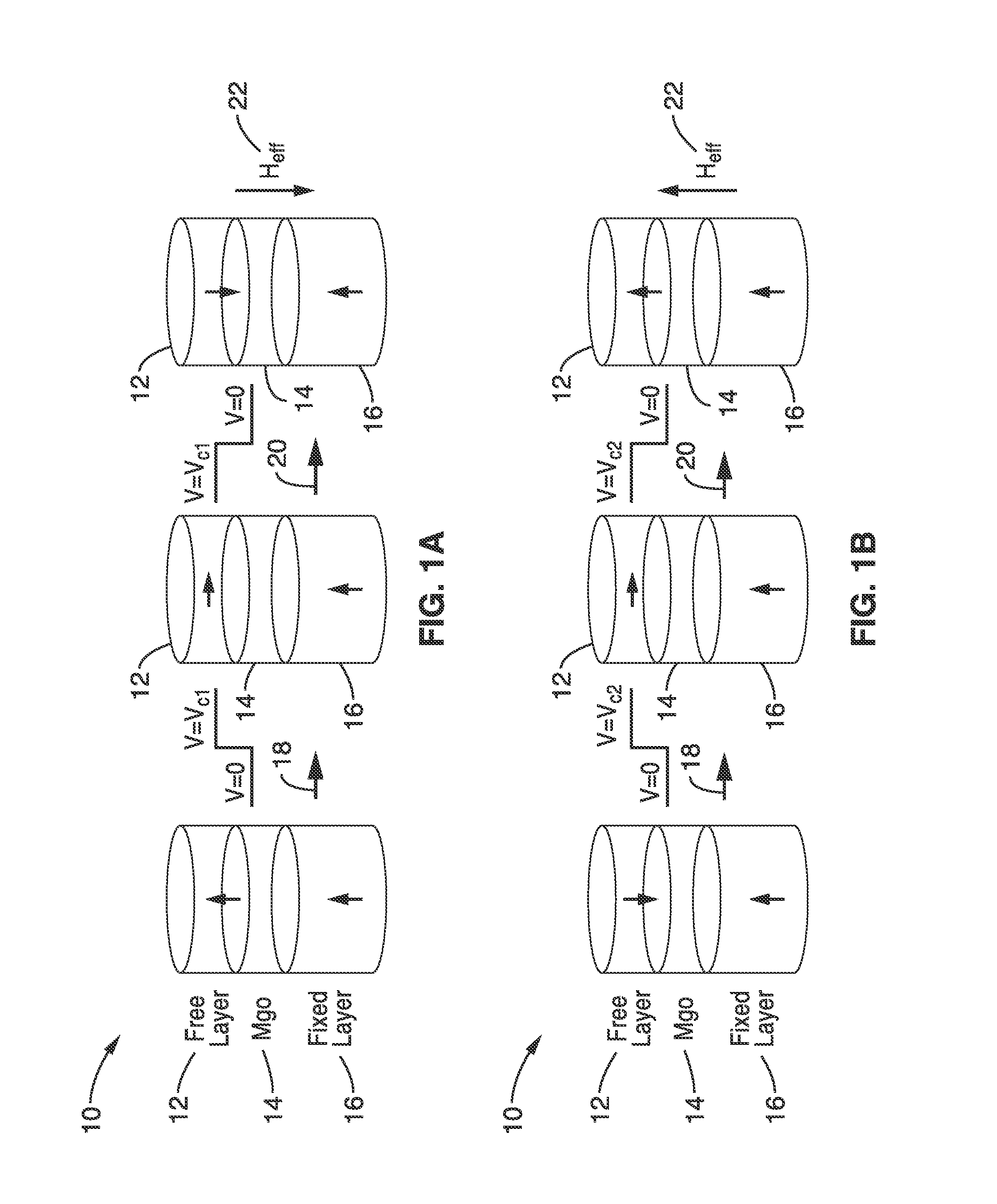
[0043]FIG. 1A and FIG. 1B illustrate MEJ switching performed from P to AP in FIG. 1A and for AP to P in FIG. 1B for out-of-plane magnetization (vertical). Each of the figures depict transition from an initial state, to an intermediate state to a final state. Similar figures could be shown for in-plane-magnetization (horizontal), as it operates in the same manner. In each of FIGS. 1A and 1B, magnetization is forced from a stable state (shown at the left of the figure) into a meta-stable state (shown in figure center) by an applied pulse voltage. Upon relaxing, the applied voltage magnetization relaxes (shown at the right) to a (similar or different) stable state. In some cases, the initial equilibrium state and the end state may include both an out-of-plane component and an in-plane component due to the compensation between in-plane shape anisotropy and out-of-plane interfacial anisotropy.
[0044]More particularly, each of the figures depict a free layer 12, in relation to a dielectric...
embodiment 110
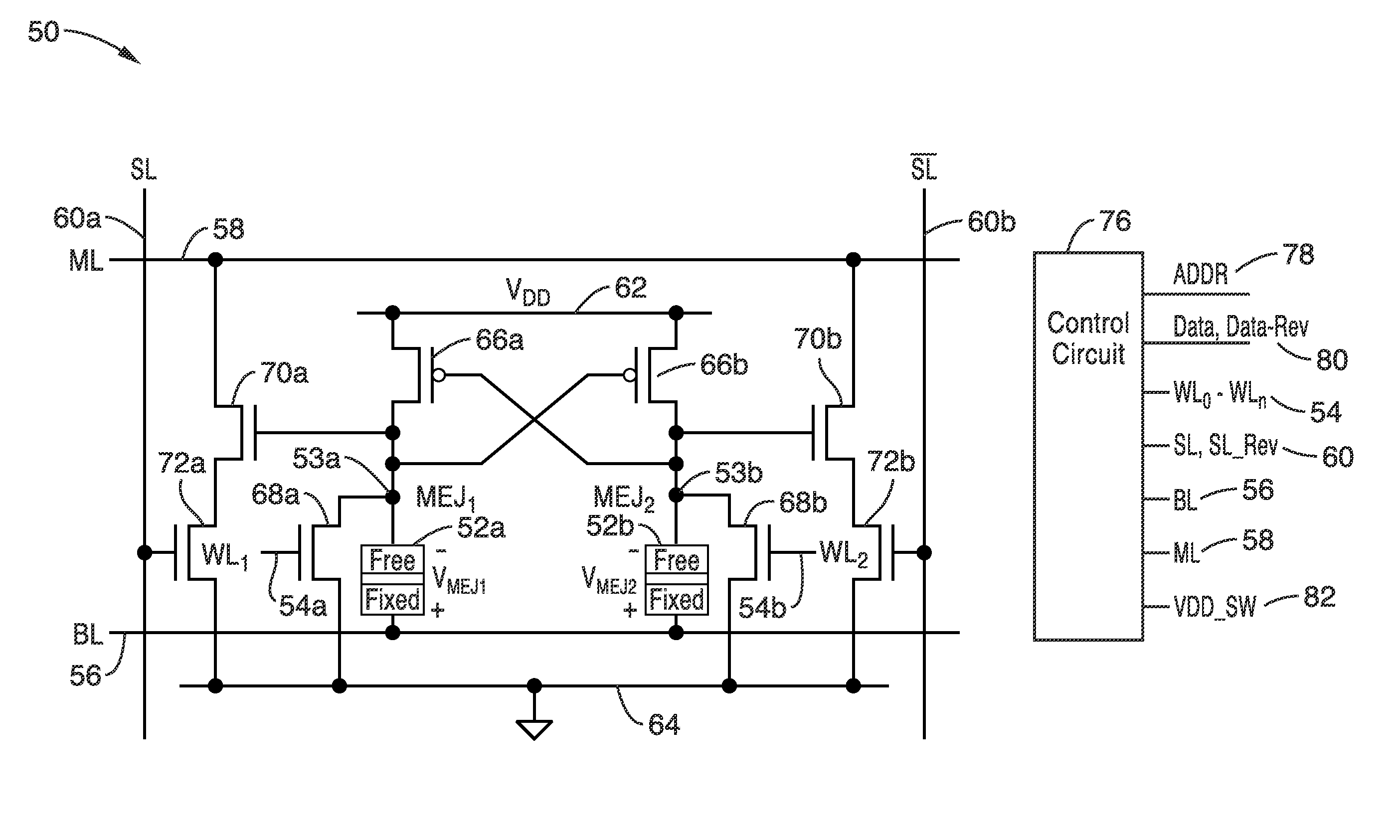
[0069]FIG. 7 illustrates overall match-line architecture, with 3-stage match-line segmentation and pipelining. Three stages 112, 114, 116 are seen in the figure, each having a given size CAM, depicted as a first stage with ×3 CAM 118, a second stage with ×7 CAM 120, and a third stage having local and global match lines with an ×11 122 and ×12 CAM 124. The global match line is ML 136, with an ML inside each of the CAM blocks 122, 124 having local match lines. The local and global match-lines are used in the third stage to reduce worst-case delay (1-bit mismatch) from approximately 1 ns to less than 200 ps. The stages are interconnected with registers 126, 128 and a register 130 at the output. It will be appreciated that the registers allow the results to be pipelined so that the CAM operates faster. The 3 stages of match line is seen in the figure as ML1 132, ML2 134 and ML3 136.
[0070]FIG. 8 illustrates a timing diagram as an HSPICE simulation of the nonvolatile, voltage-controlled, ...
PUM
 Abstract
Description
Claims
Application Information
 - R&D
- Intellectual Property
- Life Sciences
- Materials
- Tech Scout
- Unparalleled Data Quality
- Higher Quality Content
- 60% Fewer Hallucinations
Browse by: Latest US Patents, China's latest patents, Technical Efficacy Thesaurus, Application Domain, Technology Topic, Popular Technical Reports.
© 2025 PatSnap. All rights reserved.Legal|Privacy policy|Modern Slavery Act Transparency Statement|Sitemap|About US| Contact US: help@patsnap.com


