Mosfet with improved performance through induced net charge region in thick bottom insulator

Active Publication Date: 2013-12-12
ALPHA & OMEGA SEMICON INC
View PDF4 Cites 3 Cited by
  • Summary
  • Abstract
  • Description
  • Claims
  • Application Information

AI Technical Summary

Benefits of technology

The present invention provides a modification to a MOSFET structure that combines the benefits of a shielded gate transistor (SGT) without the difficulty of fabricating it. This modification involves using electron irradiation during the manufacturing process of a P-type TBO trench MOSFET. The electron irradiation step results in a RDSA (the drain-to-source voltage) of -40% less than a conventional TBO trench MOSFET, and is effective in improving the breakdown voltage and reducing RDSA, which is the trade-off between breakdown voltage and resistance. Overall, this modification simplifies the construction of the MOSFET device while achieving better performance.

Problems solved by technology

Conventional technologies to configure and manufacture high voltage semiconductor power devices are still confronted with difficulties and limitations to further improvement of device performances due to different tradeoffs.
However, a heavily doped epitaxial layer also reduces the breakdown voltage that can be sustained by the semiconductor power device.
Although the SGT provides advantages, the process of manufacturing SGT MOSFET devices is more complicated because it requires a dual poly process, in which the step of etching back the shield electrode, or poly 1, is difficult to control.
Furthermore, the SGT MOSFET structure presents challenges in forming the dielectric isolation between the shield electrode and gate electrode.

Method used


Image

  • Mosfet with improved performance through induced net charge region in thick bottom insulator
  • Mosfet with improved performance through induced net charge region in thick bottom insulator
  • Mosfet with improved performance through induced net charge region in thick bottom insulator

Examples


embodiments

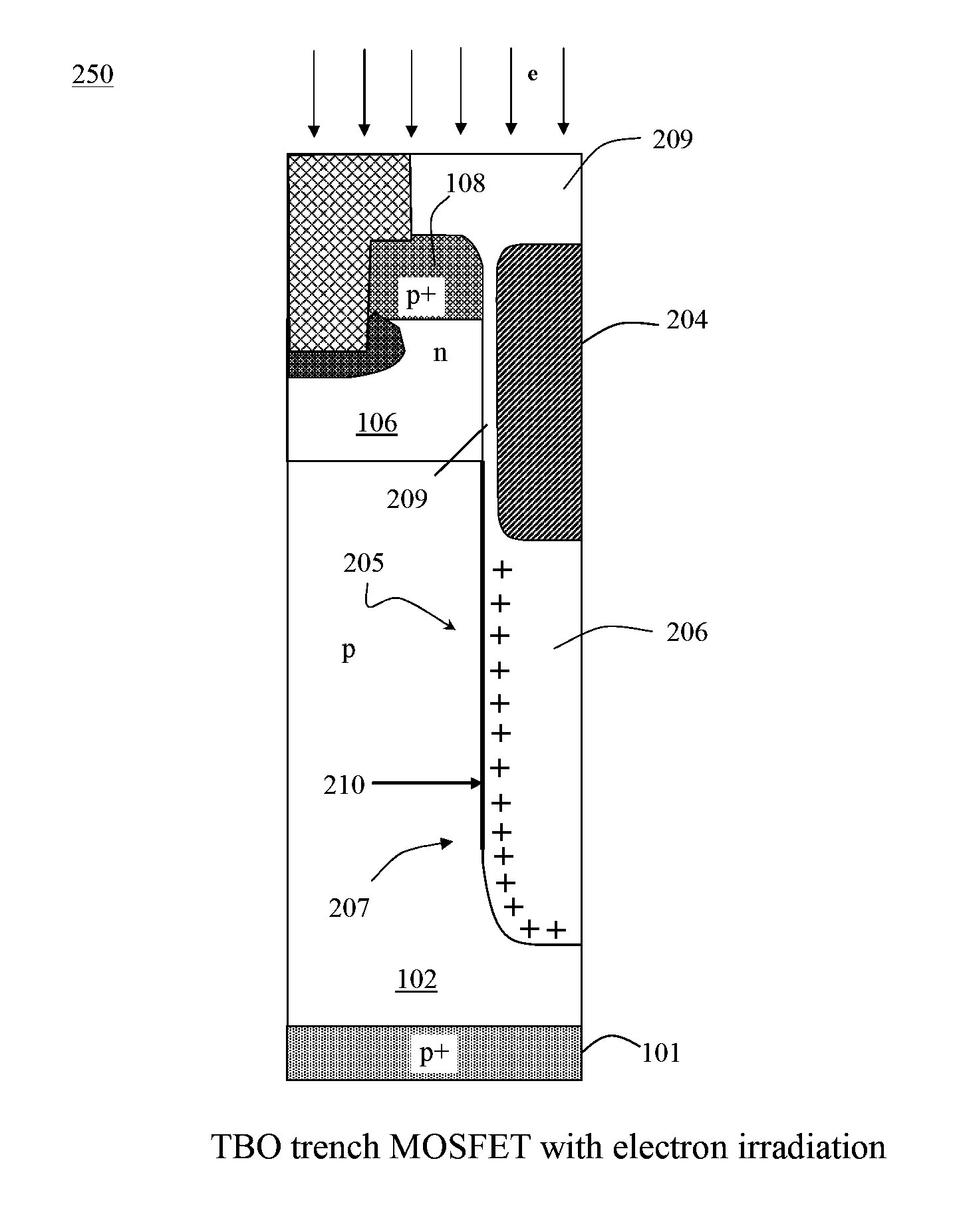
[0019]According to an embodiment of the present invention, the drift / epitaxial region 102 in a TBO MOSFET may be doped with high doping concentration to reduce the RdsA while maintain high breakdown voltage by the RESURF (reduced surface fields) effect. In general, the doping concentration is roughly two to five times the doping concentration for a conventional (unshielded) MOSFET depending on the voltage rating of the device.

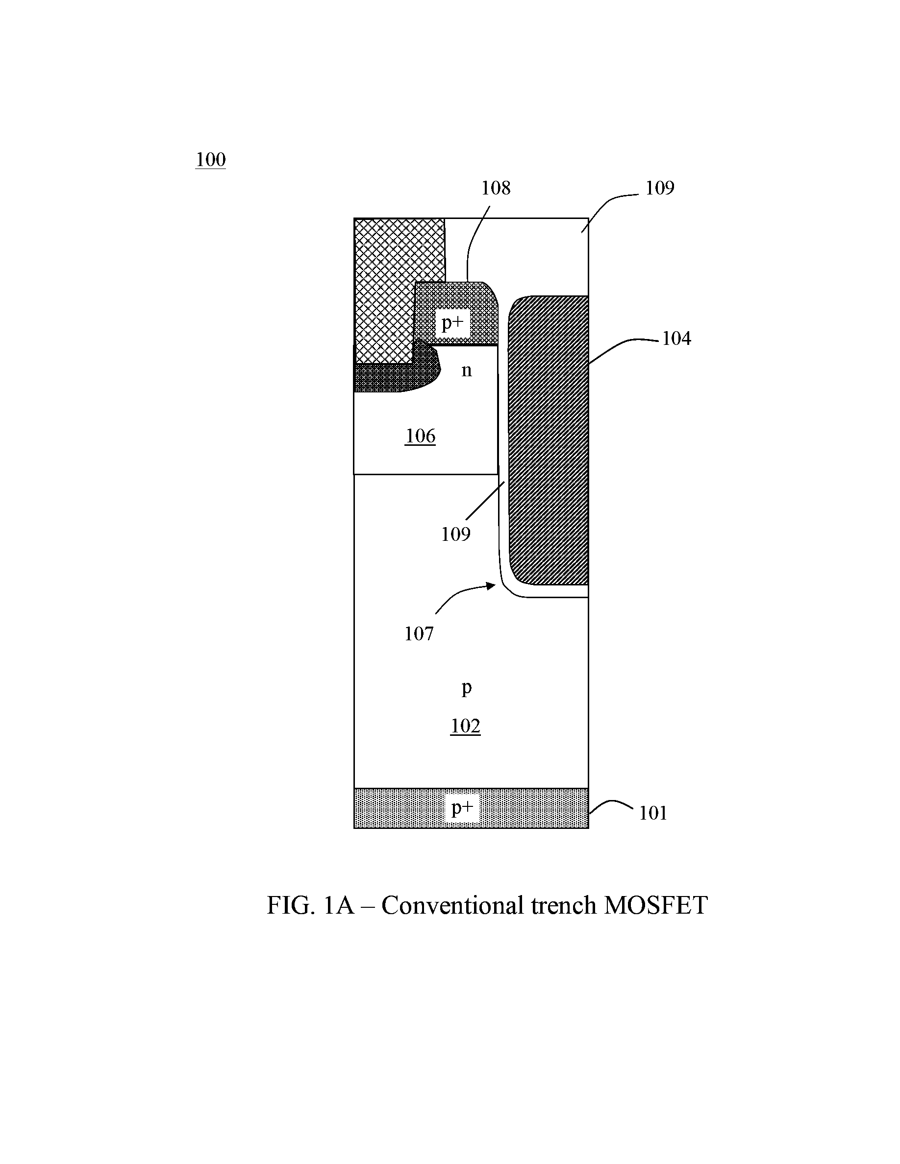
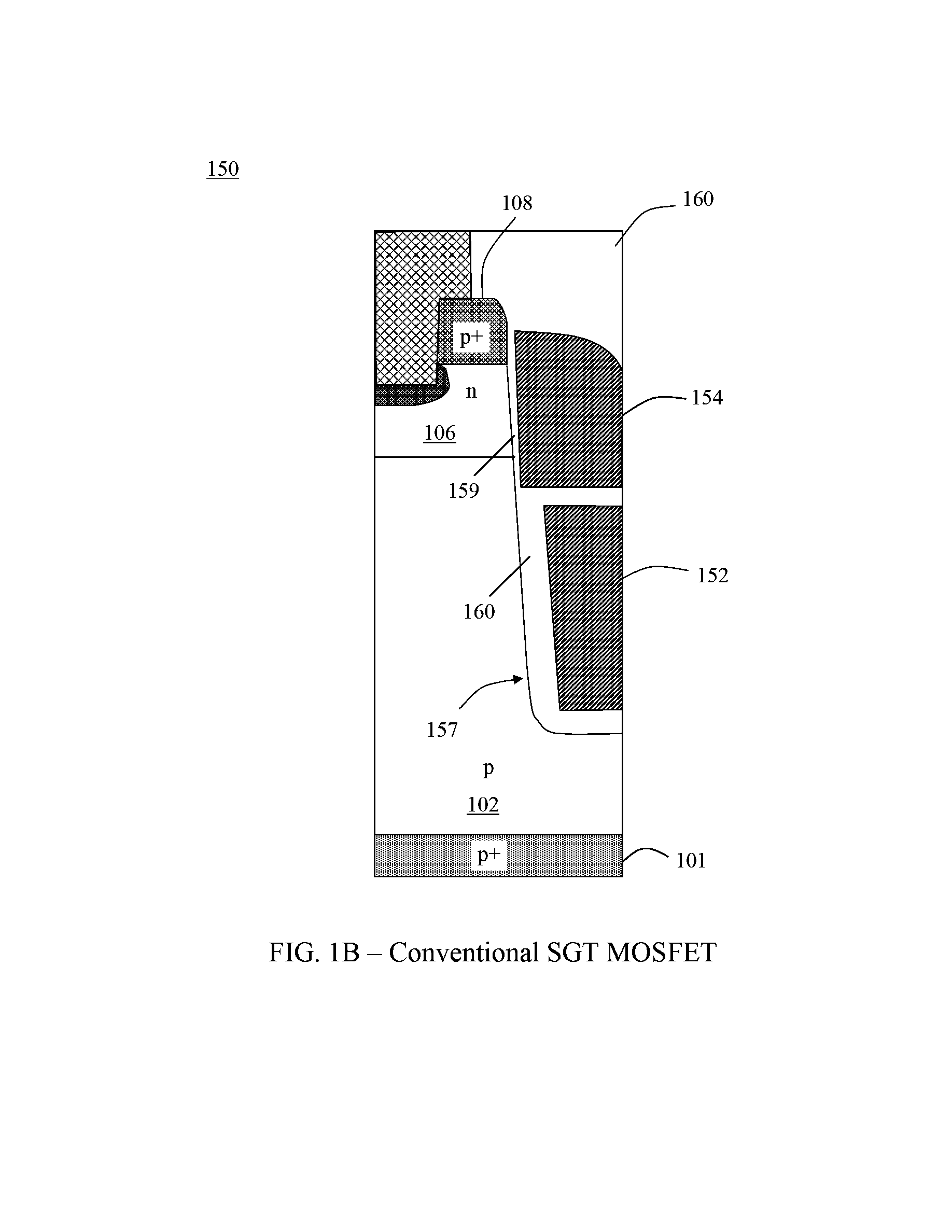
[0020]A shield electrode in an SGT, such as that shown in FIG. 1B, is a conventional way to implement the RESURF effect with a complicated double poly process. In embodiments of the present invention, by contrast, an innovative technique is presented to achieve the same RESURF effect but with much a simpler single poly process. An example of a device structure 250 formed by this technique is shown in FIG. 2B. Unlike the conventional TBO trench MOSFET 200, the dielectric material 206 underneath the gate electrode 204 is thicker, about 2 μm to 5 μm. A region of n...


PUM


Abstract

A semiconductor power device includes a thick bottom insulator formed in a lower portion of a trench in a semiconductor epitaxial region. An electrically conductive gate electrode is formed in the trench above the bottom insulator. The gate electrode is electrically insulated from the epitaxial region by the bottom insulator and a gate insulator. Charge is deliberately induced in the thick bottom insulator proximate an interface between the bottom insulator and the epitaxial semiconductor region. It is emphasized that this abstract is provided to comply with the rules requiring an abstract that will allow a searcher or other reader to quickly ascertain the subject matter of the technical disclosure. It is submitted with the understanding that it will not be used to interpret or limit the scope or meaning of the claims.

Description

FIELD OF THE INVENTION[0001]This invention relates in general to semiconductor power field effect transistor devices and in particular to thick bottom oxide (TBO) MOSFET devices with improved drain to source on-resistance.BACKGROUND OF THE INVENTIONS[0002]Conventional technologies to configure and manufacture high voltage semiconductor power devices are still confronted with difficulties and limitations to further improvement of device performances due to different tradeoffs. In vertical semiconductor power devices, there is a tradeoff between the drain to source resistance, i.e., on-resistance, commonly represented by RdsA (i.e., Rds X unit Area) as a performance characteristic, and the breakdown voltage sustainable of the power device. For the purpose of reducing the RdsA, an epitaxial layer is formed with higher dopant concentration. However, a heavily doped epitaxial layer also reduces the breakdown voltage that can be sustained by the semiconductor power device.[0003]Several de...

Claims


Application Information

Patent Timeline
IPC IPC(8): H01L29/78H01L21/336
CPCH01L29/408H01L29/41766H01L29/42368H01L29/66734H01L29/7813H01L21/42
Inventor WANG, XIAOBINBHALLA, ANUPNG, DANIEL
Owner ALPHA & OMEGA SEMICON INC
Why Eureka
Try Eureka