
Method for making light emitting diode

a technology of light-emitting diodes and methods, which is applied in the direction of semiconductor devices, electrical equipment, nanotechnology, etc., can solve the problems of reduced light-emitting from the active layer, low extraction efficiency of leds, and reduced light-emitting efficiency

Active Publication Date: 2013-10-03
TSINGHUA UNIV +1
View PDF3 Cites 4 Cited by
  • Summary
  • Abstract
  • Description
  • Claims
  • Application Information

AI Technical Summary

Benefits of technology

The patent text explains the factors that limit the extraction efficiency of LEDs, which can cause damage to the semiconductor materials and decrease the lifespan of the LED. The technical effects of the patent are to improve the extraction efficiency of LEDs and prevent damage to the semiconductor materials, which can affect their performance and lifespan. This is important for the large-scale application of LEDs.

Problems solved by technology

However, extraction efficiency of LEDs is low for the following reasons: first, the typical semiconductor materials have a higher refraction index than that of air, therefore, large-angle lights emitted from the active layer may be internally reflected in LEDs, so that a large portion of the lights emitted from the active layer will remain in the LEDs; second, the current is limited under the P-type electrode, so that the conduction of the current along a direction away from the P-type electrode is weaken, thus the lights emitted from the active layer is reduced.
Therefore, the property of the semiconductor materials is damaged and the life span of the LED is shorter.
As a result, the large-scale application of the LEDs is affected.

Method used


Image

  • Method for making light emitting diode
  • Method for making light emitting diode
  • Method for making light emitting diode

Examples


Embodiment Construction

[0023]The disclosure is illustrated by way of example and not by way of limitation in the figures of the accompanying drawings in which like references indicate similar elements. It should be noted that references to “an” or “one” embodiment in this disclosure are not necessarily to the same embodiment, and such references mean at least one.

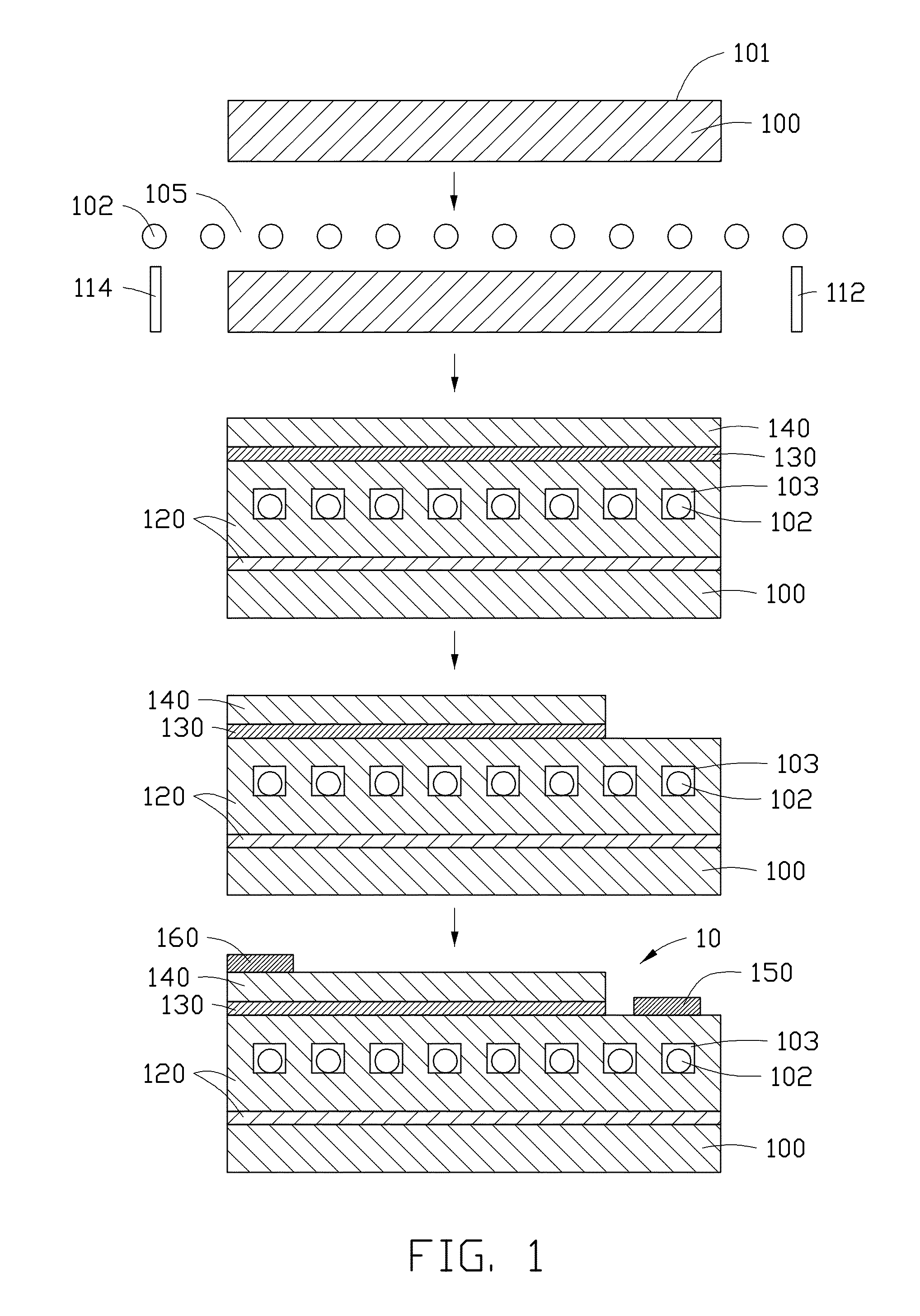
[0024]Referring to FIG. 1, a method for making an LED of one embodiment includes the following steps:

[0025]S11, providing a substrate 100 having an epitaxial growth surface 101;

[0026]S12, suspending a carbon nanotube layer 102 above the epitaxial growth surface 101; and

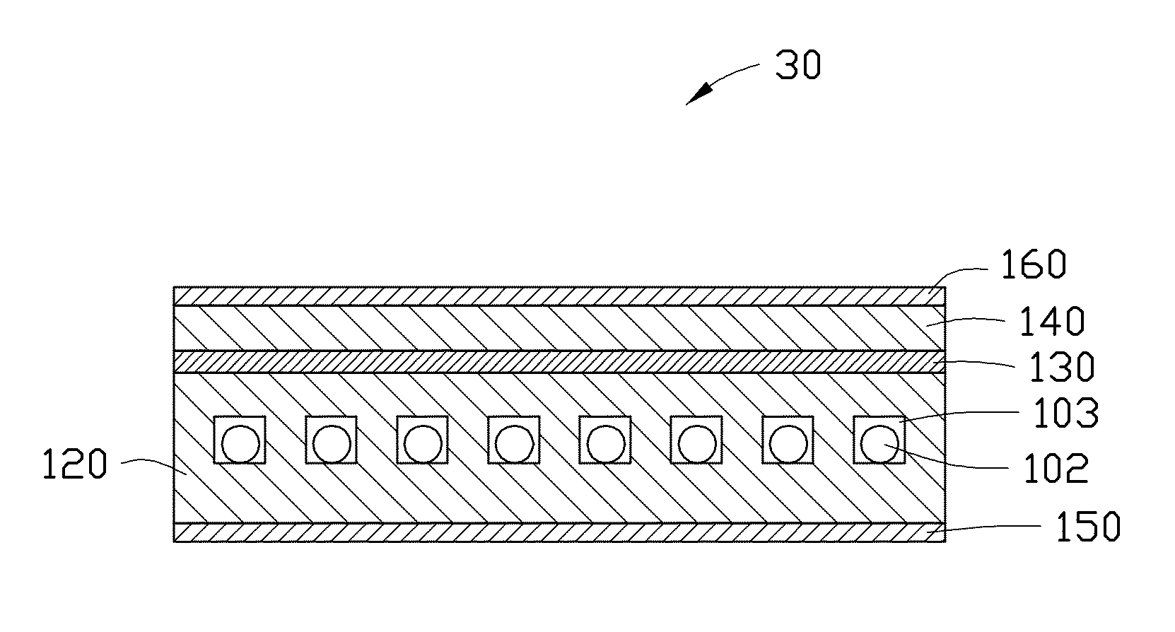
[0027]S13, growing a first semiconductor layer 120, an active layer 130, and a second semiconductor layer 140 on the epitaxial growth surface 101 in that order, in which the carbon nanotube layer 102 is enclosed in the first semiconductor layer 120;

[0028]S14, etching a portion of the second semiconductor layer 140 and the active layer 130 to expose a portion of the first semiconduc...


PUM

PropertyMeasurementUnit
widthaaaaaaaaaa
sizesaaaaaaaaaa
sizesaaaaaaaaaa

Abstract

A method for making light emitting diode, the method includes the following steps. First, a substrate having an epitaxial growth surface is provided. Second, a carbon nanotube layer is suspended above the epitaxial growth surface. Third, a first semiconductor layer, an active layer and a second semiconductor layer are grown on the epitaxial growth surface in that order, wherein the first semiconductor layer includes a buffer layer, an intrinsic semiconductor layer, and a doped semiconductor layer stacked in that order. Fourth, the doped semiconductor layer is exposed by removing the substrate, the buffer layer, and the intrinsic semiconductor layer. Fifth, a first electrode is prepared on the first semiconductor layer and a second electrode is prepared on the second semiconductor layer.

Description

CROSS-REFERENCE TO RELATED APPLICATIONS[0001]This application is a continuation of U.S. patent application Ser. No. 13 / 288,213, filed on Nov. 3, 2011, entitled, “METHOD FOR MAKING LIGHT EMITTING DIODE,” which claims all benefits accruing under 35 U.S.C. §119 from China Patent Application No. 201110110728.6, filed on Apr. 29, 2011 in the China Intellectual Property Office. The disclosures of the above-identified applications are incorporated herein by reference.BACKGROUND[0002]1. Technical Field[0003]The present disclosure relates to a light emitting diode (LED) and method for making the same.[0004]2. Description of Related Art[0005]In recent years, highly efficient LEDs made with GaN-based semiconductors have become widely used in different technologies, such as in display devices, large electronic bill boards, street lights, car lights, and other illumination applications. LEDs are environmentally friendly, long working life, and low power consumption.[0006]A conventional LED commo...

Claims


Application Information

Patent Timeline
Patent Type & Authority Applications(United States)
IPC IPC(8): H01L33/36H01L33/64
CPCH01L21/02521H01L33/0062H01L21/02546H01L21/02579H01L21/0262H01L21/02642H01L21/02647H01L33/007H01L33/641H01L21/0237H01L21/0242H01L21/02458H01L51/0048B82Y40/00H01L33/36H01L33/64Y10S977/742H01L33/20H01L2924/0002H01L21/0254B82Y10/00H01L2924/00H10K85/221
Inventor WEI, YANGFAN, SHOU-SHAN
Owner TSINGHUA UNIV
Learn More