Patterned substrate and stacked light emitting diode

a light-emitting diode and substrate technology, applied in the field of semiconductor structure, can solve the problems of affecting the current transmitting path and achieve the effect of improving crystal quality and crystal quality

Inactive Publication Date: 2013-08-01
LEXTAR ELECTRONICS CORP
View PDF4 Cites 15 Cited by
  • Summary
  • Abstract
  • Description
  • Claims
  • Application Information

AI Technical Summary

Benefits of technology

The invention provides a way to make a better quality epitaxial layer for LEDs, which can help improve their performance and reduce defects. This is achieved through the use of a patterned substrate and other techniques that enhance the growth of the epitaxial layer.

Problems solved by technology

Most of the modern advanced semiconductor electronic devices and electric optical device are fabricated by growth and stacking of epitaxy as a crystal, and a substrate is a key issue for the epitaxial growth of semiconductor structure in the devices.
However, the masks are all formed in the semiconductor layer and a current transmitting path will be thus affected.

Method used


Image

  • Patterned substrate and stacked light emitting diode
  • Patterned substrate and stacked light emitting diode
  • Patterned substrate and stacked light emitting diode

Examples


Embodiment Construction

[0023]The following description is of the best-contemplated mode of carrying out the invention. This description is made for the purpose of illustrating the general principles of the invention and should not be taken in a limiting sense. The scope of the invention is best determined by reference to the appended claims.

[0024]FIGS. 1-27 illustrate fabrications of a stacked light emitting device structure according to various embodiments of the invention.

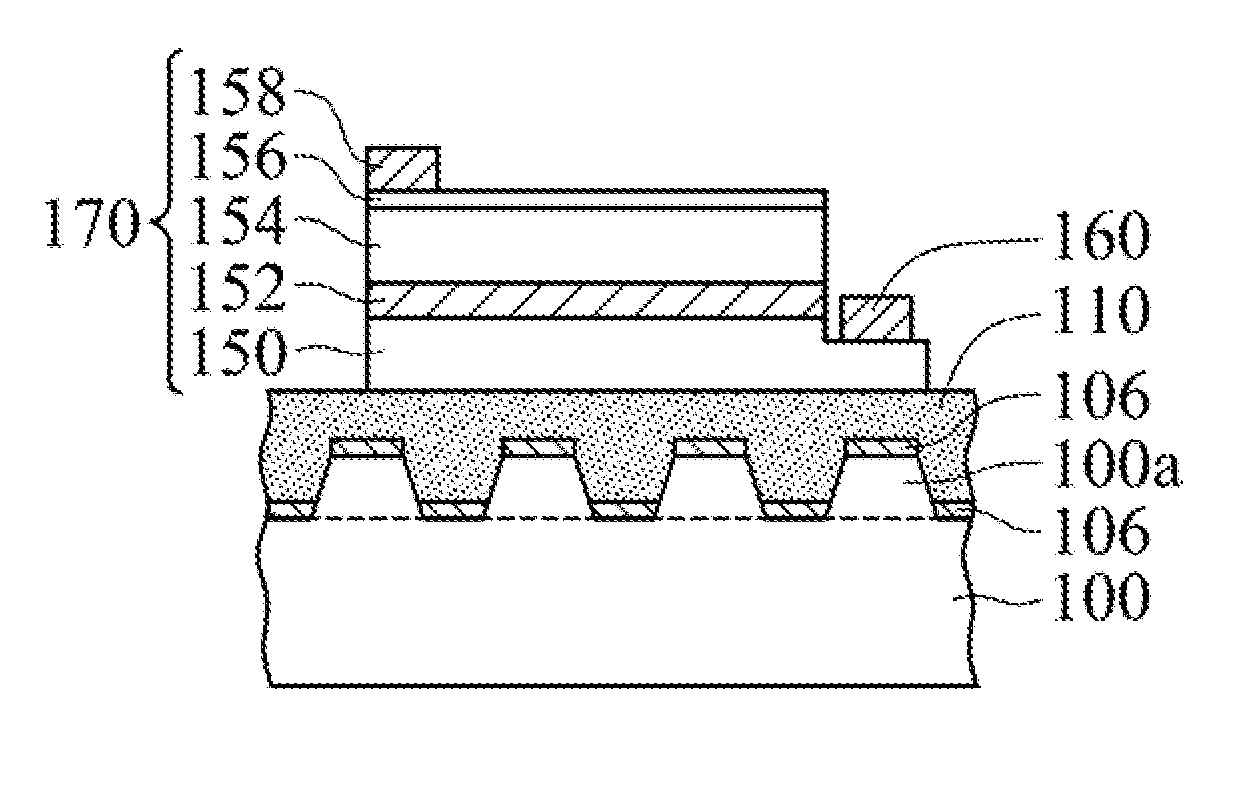
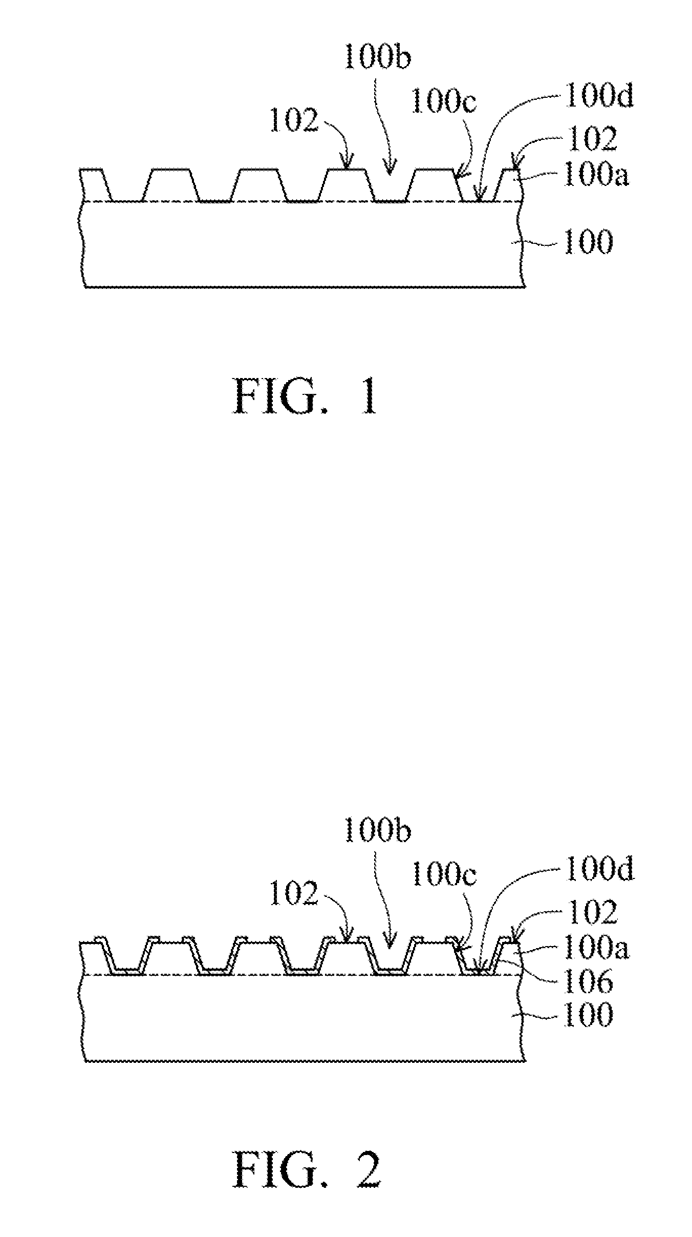
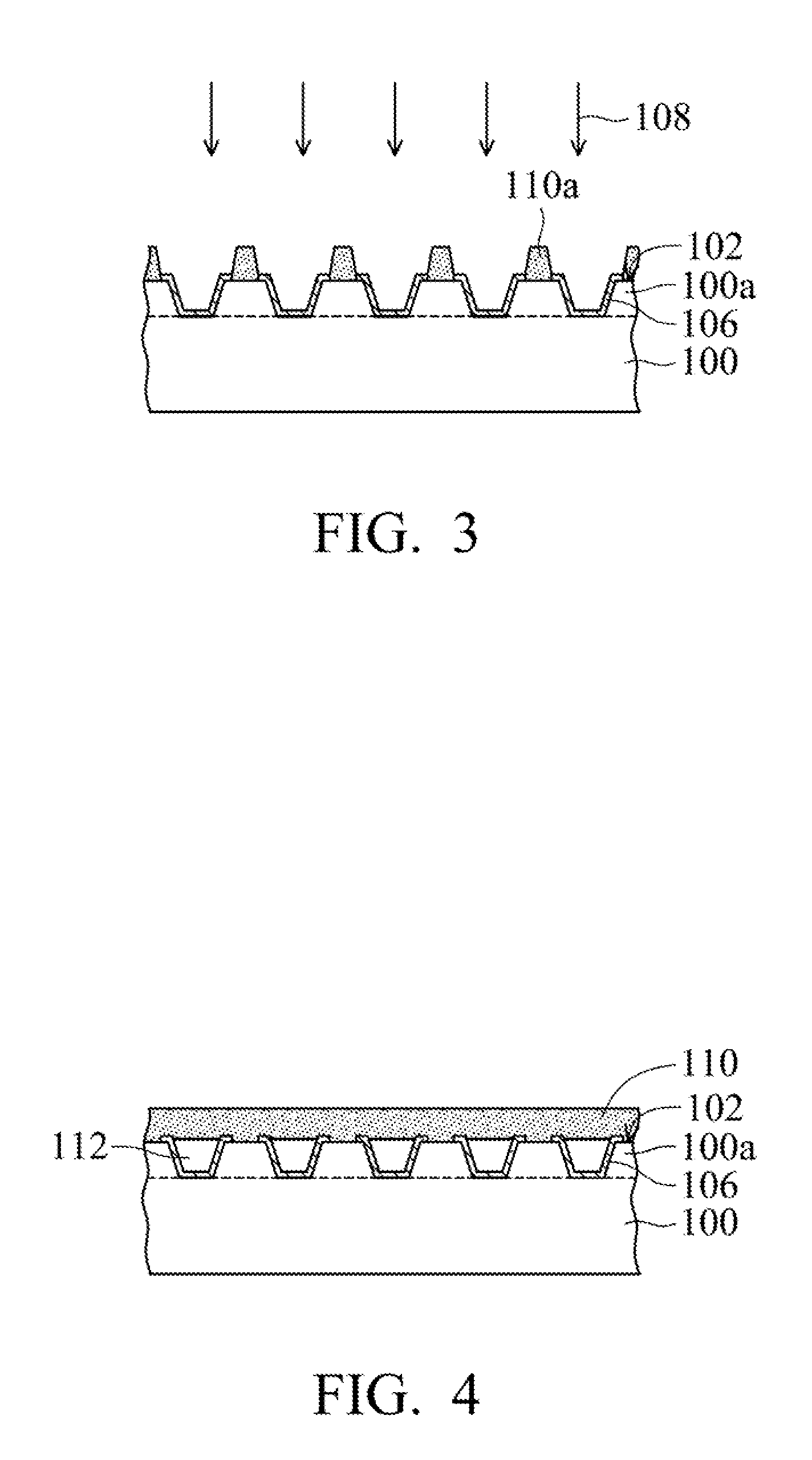
[0025]Referring to FIGS. 1-5, a manufacturing process of a stacked LED structure is shown according to an embodiment of the invention. Referring to FIG. 1, a substrate 100 with a flat surface is provided first, such as the sapphire substrate, having a top surface 102 which is substantially a flat surface. The material of the substrate 100 may include sapphire, silicon, silicon carbide and so on. Then, by applying a suitable patterned mask (not shown), the photolithography is used to define an etching area, and then by implementing an e...


PUM


Abstract

A patterned substrate is provided, including: a substrate having a (0001) crystal plane and a plurality of alternatively arranged recess structures therein, thereby forming a plurality of alternatively arranged top surfaces; and a dielectric barrier layer covering the bottom surface and / or the sidewalls of the recess structures. Each of the alternatively arranged recess structures includes a bottom surface and a plurality of sidewalls surrounding the bottom surface.

Description

RELATED APPLICATIONS[0001]This application claims priority of Taiwan Patent Application No. 101102782, filed on Jan. 30, 2012, the entirety of which is incorporated by reference herein.BACKGROUND[0002]1. Technical Field[0003]The present invention relates to a semiconductor structure and a method for fabricating the same, and in particularly to a method for fabricating a patterned substrate with epitaxial layers having improved crystal quality and stacked semiconductor structures with epitaxial layers having improved crystal quality.[0004]2. Description of the Related Art[0005]Light emitting diode (LED) is one of the most applied semiconductor devices in recent years, for having characteristics such as low power consumption, low pollution, and long lifetime. As such, the LED can be used in such as traffic lights, outdoor displays, and back light modules for displays.[0006]Most of the modern advanced semiconductor electronic devices and electric optical device are fabricated by growth...

Claims


Application Information

Patent Timeline
IPC IPC(8): H01L29/04H01L29/12H01L33/02H01L29/16
CPCC30B25/18H01L33/02H01L29/12C30B15/00H01L33/007C30B29/06H01L29/1608H01L29/04
Inventor CHOU, HSIU-MEICHEN, JUN-RONGYE, JHAO-CHENG
Owner LEXTAR ELECTRONICS CORP
Why Eureka
Try Eureka