
Pll circuit

a circuit and phase noise technology, applied in the field of digital wireless systems, can solve the problems of code error, high phase noise level of rf lo signal, increased cost, etc., and achieve the effect of stable operation

Inactive Publication Date: 2013-07-18
NEC CORP
View PDF2 Cites 8 Cited by
  • Summary
  • Abstract
  • Description
  • Claims
  • Application Information

AI Technical Summary

Benefits of technology

The invention allows for stable operation of demodulator functions even at low C / N values. This means that the device can recover carriers and synchronize with clocks effectively even at low signal-to-noise ratios.

Problems solved by technology

Therefore, in a millimeter wave or microwave wireless system in which the RF frequency is several GHz to several tens of GHz, the phase noise level of the RF LO signal is very high.
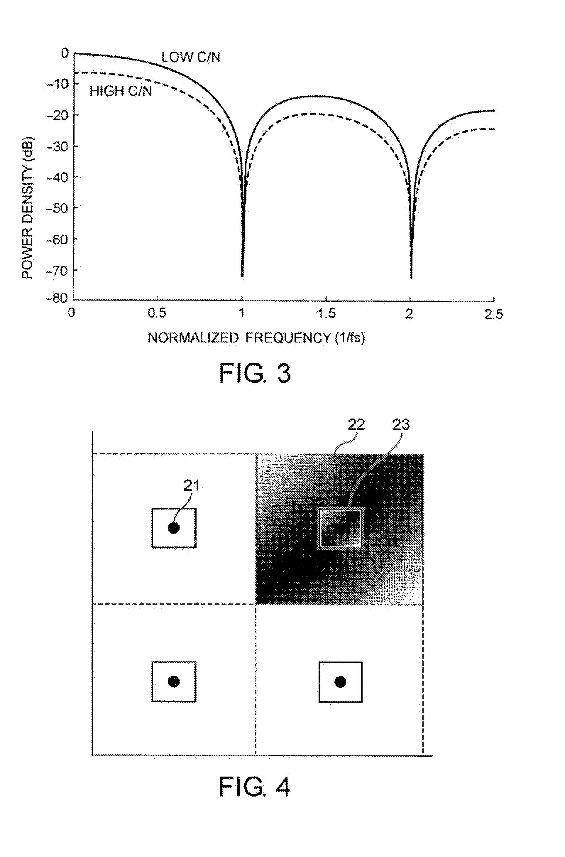
Thus, a code error occurs when the deviation exceeds a threshold with respect to an adjacent constellation point.
Reducing the phase noise level of an LO signal, however, leads to increased cost and narrows the frequency variable range of a transceiver.
The first problem is that the suppression effect needs to be enhanced because the phase noise level is high.
The second problem is that there is an adverse influence on the stable operation in a low C / N environment.
First, the problem in carrier recovery is described.
However, in the case of using a multilevel QAM having more severe BER characteristics or using high-gain error correction, there are adverse influences on the stable operation of the demodulator and the BER improving effect by error correction.
This is responsible for fluctuations in clock phase control, resulting in increased clock jitter.
However, from the mutual bandwidth relationship among a plurality of PLL circuits for clock rate conversion arranged on the transmission side or on the downstream of the demodulator on the reception side, the bandwidth of only a PLL circuit for clock synchronization in the demodulator cannot be narrowed.
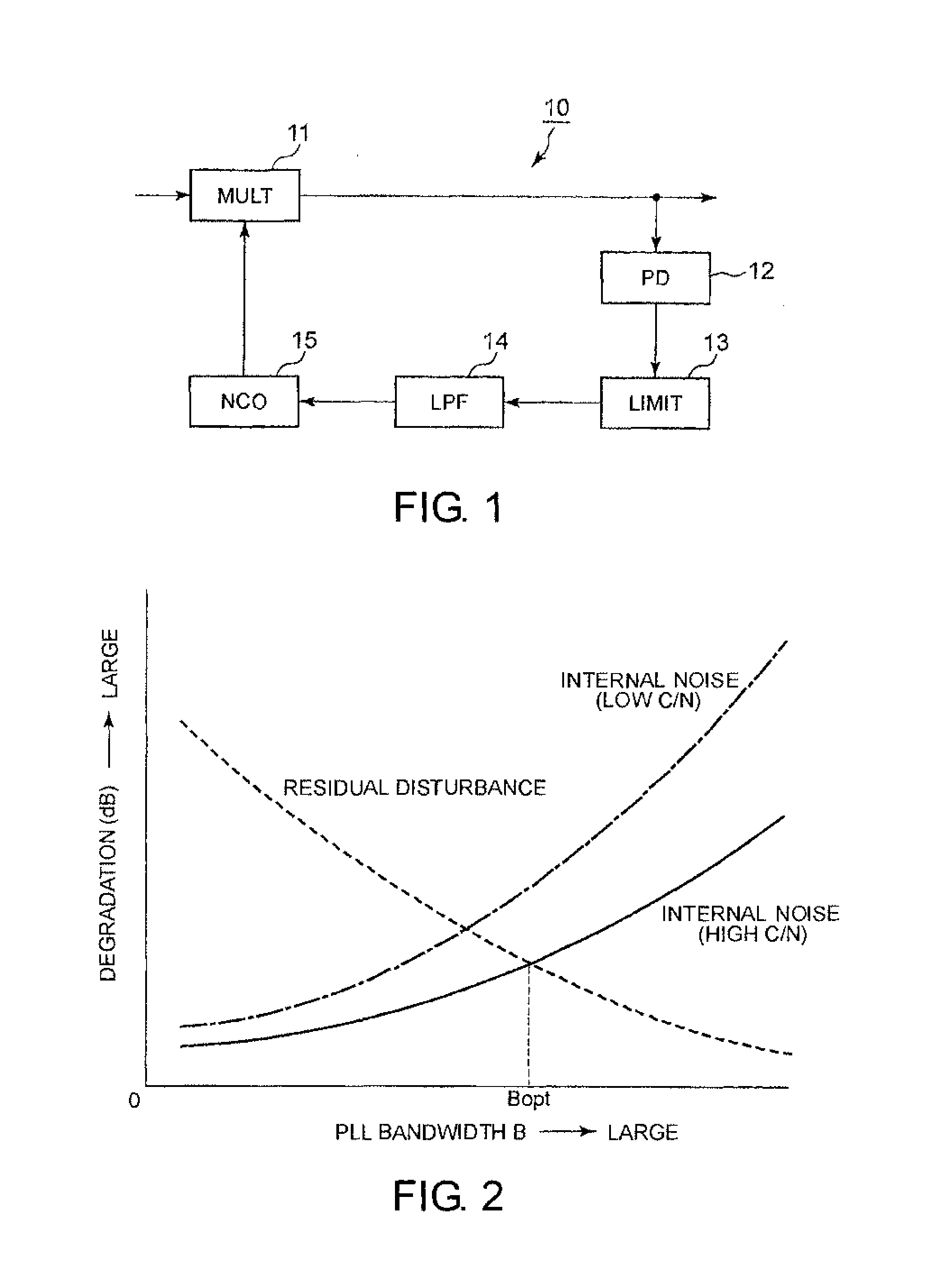
As described above, both in the carrier recovery and in the clock synchronization, the optimum value of the bandwidth B of the PLL circuit is determined in view of both the elements of enlarging and narrowing the bandwidth B. In recent years, conditions that make it difficult to achieve both the elements have been required, and it has been difficult to determine the optimum value.
This problem is unavoidable in the case where a well-known, basic PLL circuit is operated under a wide bandwidth and low C / N environment.
(2) Processing on the demodulator side is formed of an analog stage before A / D conversion, which is not suitable for a device having a highly-digitized circuit.
Therefore, in Patent Literature 2, the synchronization determination circuit or the C / N determination circuit, and the selector are necessary, leading to a problem of a complicated configuration.
Patent Literature 2 has another problem in that a complicated operation (calculation) is necessary because the phase comparator (phase error detection means) detects the phase by the inverse characteristics of TAN.

Method used


Image

  • Pll circuit
  • Pll circuit
  • Pll circuit

Examples


Embodiment Construction

[0035]In order to facilitate the understanding of this invention, the prior art and its problems are first described in detail. Note that, the prior art mentioned herein is the well-known, most basic PLL circuit. This is because there is no other well-known technology effective both for carrier recovery and for clock synchronization than the most basic PLL circuit.

[0036]As described above, both in carrier recovery and in clock synchronization which are main signal processing performed in a demodulator, information to be extracted is not explicitly transmitted from the transmission side. It is therefore necessary to recover the carrier and clock signals based on a result of demodulating a received signal and synchronize the recovered carrier to the frequency and phase on the transmission side. This control is thus affected by BER characteristics at the time of demodulation or by noise superimposed on constellation points.

[0037]The influence is described below.

[0038]Referring to FIG. ...


PUM


Abstract

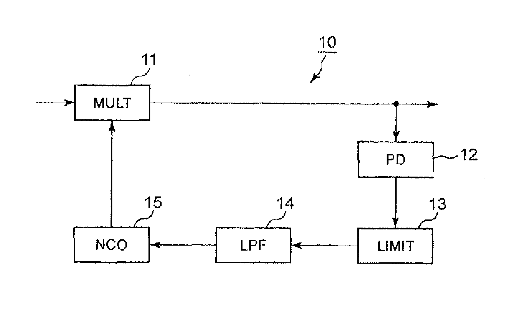
A PLL circuit, for extracting phase error information from a demodulated signal in which a variance of a phase or an amplitude changes depending on a signal-to-noise power ratio, and providing negative feedback control, to thereby suppress a phase error of the demodulated signal, includes: a phase error detector for producing a phase error signal corresponding to a value of the phase error as the phase error information; a limiter circuit for limiting an expression range of the phase error signal to a constant value or less to produce the limited phase error signal; and a loop filter for producing a control signal based on the limited phase error signal to determine frequency characteristics.

Description

TECHNICAL FIELD [0001]This invention relates to a digital wireless system, and more particularly, to a PLL circuit for use in a multilevel quadrature amplitude modulation (QAM) demodulator.BACKGROUND ART [0002]In recent years, in a digital wireless system for millimeter waves or microwaves, which is in rapidly increasing demand as a component in a mobile communication system, a multilevel quadrature amplitude modulation (QAM) scheme capable of high-capacity transmission and easy digitalization of a modulator / demodulator circuit is used as the modulation scheme.[0003]An RF local oscillator (LO) signal, which is used for frequency conversion between an intermediate frequency (IF) signal and a radio frequency (RF) signal, has phase noise. In general, the level of the phase noise (represented by power density ratio at frequency deviated from center frequency (for example, 100 kHz offset) to power density at center frequency) becomes higher as the frequency of the LO signal becomes highe...

Claims


Application Information

Patent Timeline
IPC IPC(8): H03L7/08
CPCH03L7/0807H04L27/0014H03L7/091H04L2027/0067H03L7/08H04L27/38
Inventor SASAKI, EISAKU
Owner NEC CORP
Learn More