
Chip inductor and method for manufacturing the same

Active Publication Date: 2013-06-27
SAMSUNG ELECTRO MECHANICS CO LTD
View PDF10 Cites 11 Cited by
  • Summary
  • Abstract
  • Description
  • Claims
  • Application Information

AI Technical Summary

Benefits of technology

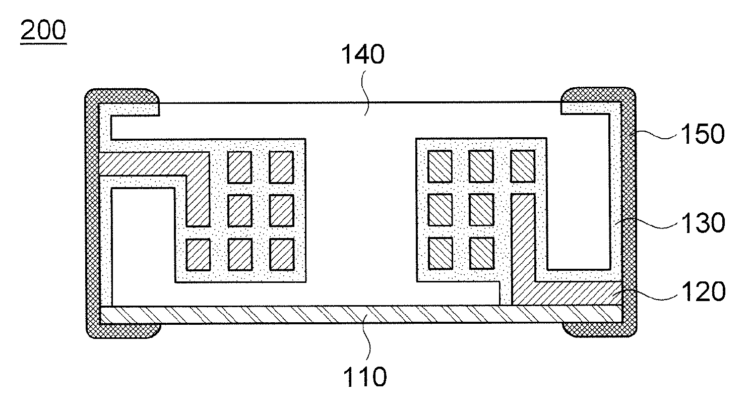
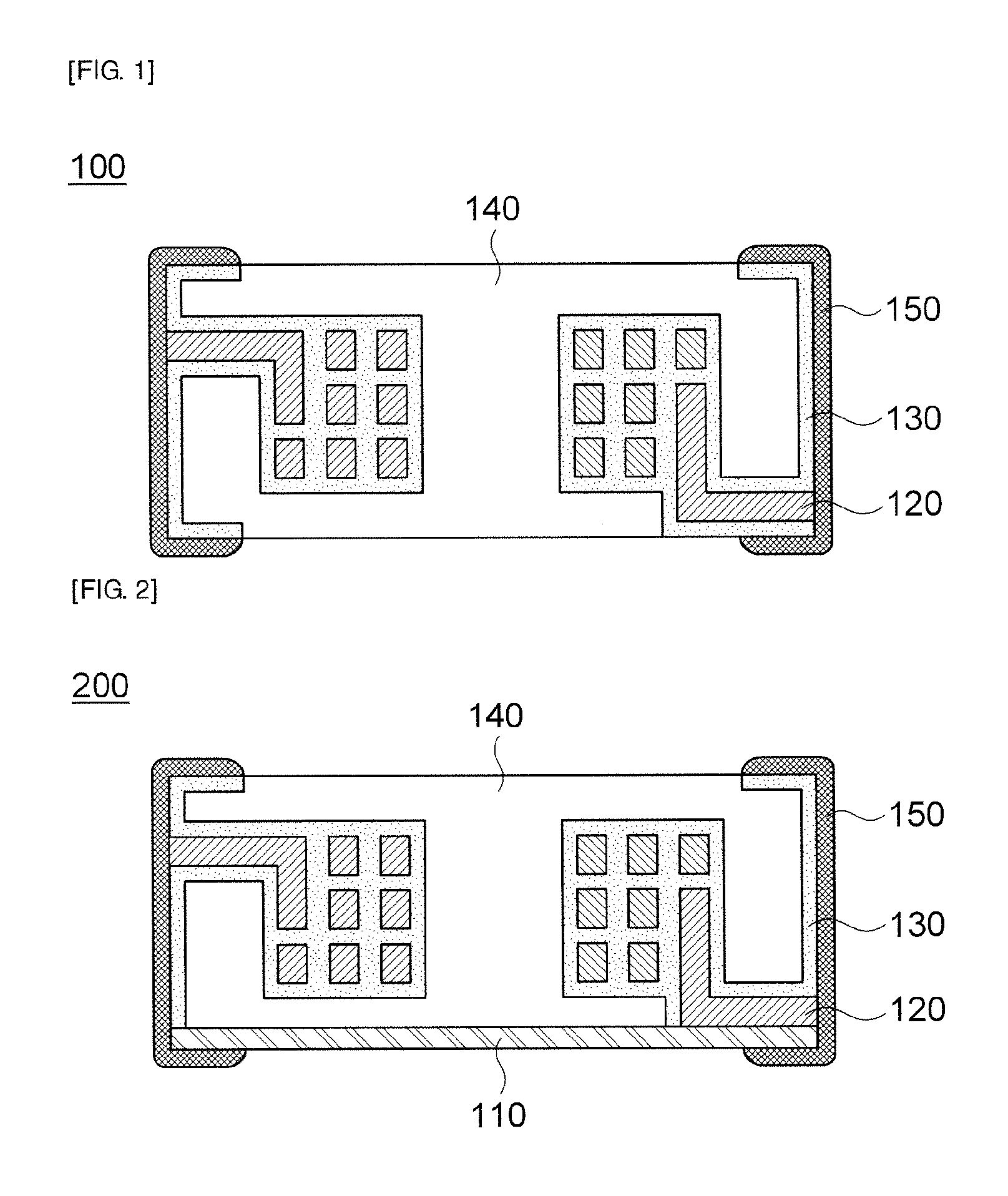
The present invention aims to provide a chip inductor that can be made smaller and thinner in a mass-production manner while improving its characteristics to overcome magnetic saturation. The invention also provides a method for manufacturing this chip inductor. The insulating portion can be formed by removing the uncured region after exposing through a mask, which exposes the region in which the wiring pattern is formed. This removal can be done to cure the exposed region. Additionally, the insulating portion can be formed by removing the region of the insulating layer except the region in which the wiring pattern is formed, and the region in which a via hole is to be formed. This helps in avoiding magnetic saturation and improving the overall performance of the chip inductor.

Problems solved by technology

However, in the conventional inductor as disclosed in the Patent Document 1, since the wiring pattern is formed on the magnetic sheet, there is a need for wiring spacing above a predetermined level due to limitations in securing insulation and processing.

Method used


Image

  • Chip inductor and method for manufacturing the same
  • Chip inductor and method for manufacturing the same
  • Chip inductor and method for manufacturing the same

Examples


Embodiment Construction

[0042]Advantages and features of the present invention and methods of accomplishing the same will be apparent by referring to embodiments described below in detail in connection with the accompanying drawings. However, the present invention is not limited to the embodiments disclosed below and may be implemented in various different forms. The embodiments are provided only for completing the disclosure of the present invention and for fully representing the scope of the present invention to those skilled in the art. Like reference numerals refer to like elements throughout the specification.

[0043]Terms used herein are provided to explain embodiments, not limiting the present invention. Throughout this specification, the singular form includes the plural form unless the context clearly indicates otherwise. When terms “comprises” and / or “comprising” used herein do not preclude existence and addition of another component, step, operation and / or device, in addition to the above-mentione...


PUM

PropertyMeasurementUnit
Diameteraaaaaaaaaa

Abstract

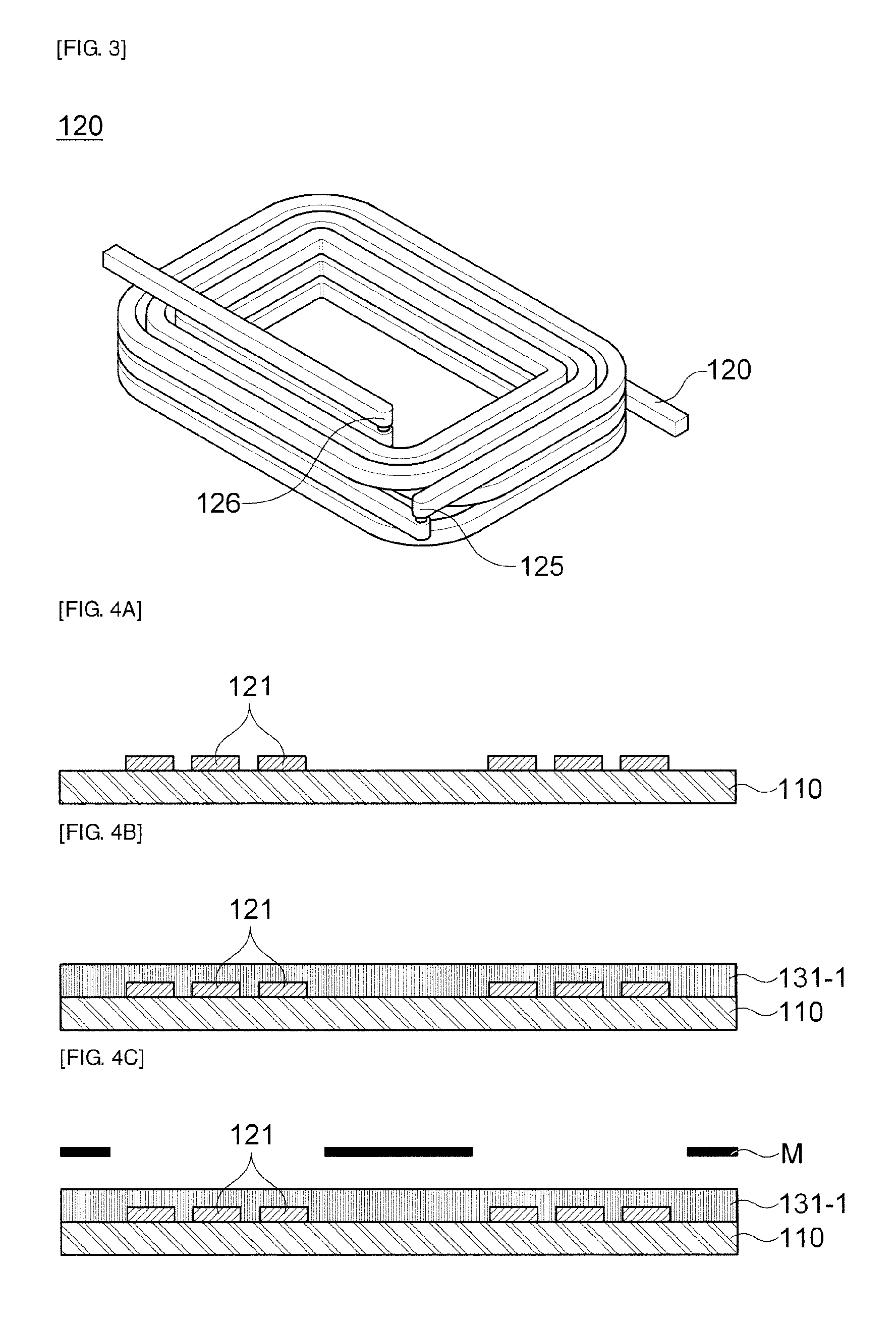
The present invention relates to a chip inductor including: a metal-polymer composite in which metal particles and polymer are mixed; a wiring pattern provided inside the metal-polymer composite to form a coil; an external electrode provided in a portion of an outer peripheral surface of the metal-polymer composite; and an insulating portion provided between the metal-polymer composite and the wiring pattern and between the metal-polymer composite and the external electrode, and a method for manufacturing the same.

Description

CROSS-REFERENCE TO RELATED APPLICATIONS[0001]Claim and incorporate by reference domestic priority application and foreign priority application as follows:[0002]CROSS REFERENCE TO RELATED APPLICATION[0003]This application claims the benefit under 35 U.S.C. Section 119 of Korean Patent Application Serial No. 10-2011-0140409, entitled filed Dec. 22, 2011, which is hereby incorporated by reference in its entirety into this application.BACKGROUND OF THE INVENTION[0004]1. Field of the Invention[0005]The present invention relates to a chip inductor and a method for manufacturing the same, and more particularly, to a chip inductor capable of removing noises by being provided in IT devices, and a method for manufacturing the same.[0006]2. Description of the Related Art[0007]In recent times, miniaturization and thinning of IT devices such as various communication devices or display devices have been accelerated, and researches for miniaturization and thinning of various devices employed in th...

Claims


Application Information

Patent Timeline
IPC IPC(8): H01F27/29H01F41/04
CPCH01F27/29H01F41/041Y10T29/4902H01F27/292H01F41/046H01F17/0033H01F5/00H01F17/00H01F27/28
Inventor CHA, HYE YEONHUR, KANG HEONPARK, SUNG JINJEONG, DONG JINPARK, JUNG MINSHIN, HYEOG SOOAN, SUNG YONGLEE, HWAN SOOKWEON, YOUNG DOHAHN, JIN WOO
Owner SAMSUNG ELECTRO MECHANICS CO LTD
Learn More