Semiconductor device, semiconductor package, interposer, semiconductor device manufacturing method and interposer manufacturing method

a semiconductor and semiconductor technology, applied in the manufacture of printed circuits, printed circuit aspects, basic electric elements, etc., can solve the problems of wire disconnection and difficulty in the above two conventional techniques, and achieve the effect of reducing the possibility of disconnection of interconnect wires passing between external coupling terminals in the interposer

Active Publication Date: 2012-11-29
RENESAS ELECTRONICS CORP
View PDF7 Cites 1 Cited by
  • Summary
  • Abstract
  • Description
  • Claims
  • Application Information

AI Technical Summary

Benefits of technology

[0010]According to the present invention, the possibility of disconnection of an interconnect wire passing between external coupling terminals in an interposer is reduced.

Problems solved by technology

If the temperature of a semiconductor device in which a semiconductor package is mounted over a printed wiring board changes, thermal stress generated due to the difference in thermal expansion coefficient between the printed wiring board and semiconductor package may affect a solder ball and cause a crack in the joint of the solder ball and an external coupling terminal of the package substrate or printed wiring board, resulting in a disconnection.
However, the present inventors have found that a difference in thermal expansion coefficient as mentioned above may cause cracking in a solder resist layer covering the surface of an interposer between external coupling terminals and such cracking may lead to a wire disconnection.
The inventors have also found it difficult for the above two conventional techniques to prevent disconnection of an interconnect wire passing between external coupling terminals.

Method used


Image

  • Semiconductor device, semiconductor package, interposer, semiconductor device manufacturing method and interposer manufacturing method
  • Semiconductor device, semiconductor package, interposer, semiconductor device manufacturing method and interposer manufacturing method
  • Semiconductor device, semiconductor package, interposer, semiconductor device manufacturing method and interposer manufacturing method

Examples


first embodiment

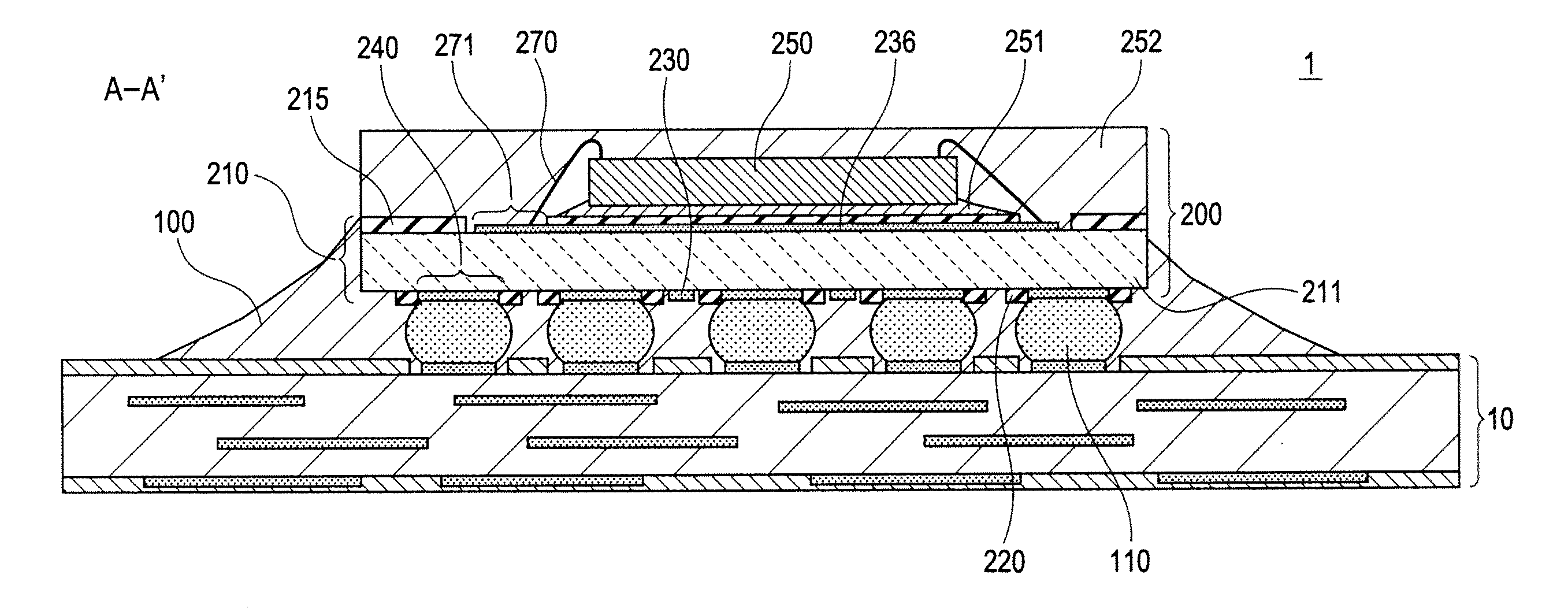
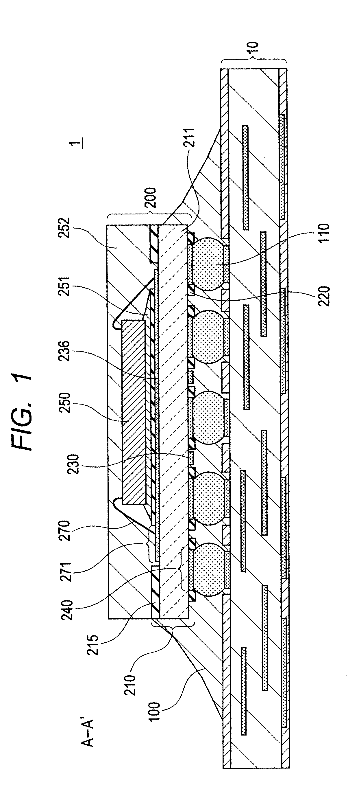
[0021]FIG. 1 is a sectional view showing the structure of a semiconductor device 1 according to the invention. The semiconductor device 1 includes an interconnection substrate 10, a semiconductor package 200, and an underfill resin layer 100. The semiconductor package 200 includes a semiconductor chip 250 and an interposer 210. The interposer 210 has the semiconductor chip 250 mounted over one surface thereof and a plurality of external coupling terminals 240 and an interconnect wire 230 formed over the other surface and is covered by a solder resist layer 220. The semiconductor package 200 is mounted over the interconnection substrate 10, for example, through solder balls 110. The underfill resin layer 100 seals the space between the semiconductor package 200 and interconnection substrate 10. In an area where the interconnect wire 230 passing between two neighboring external coupling terminals 240 intersects with a line connecting the centers of the neighboring external coupling te...

second embodiment

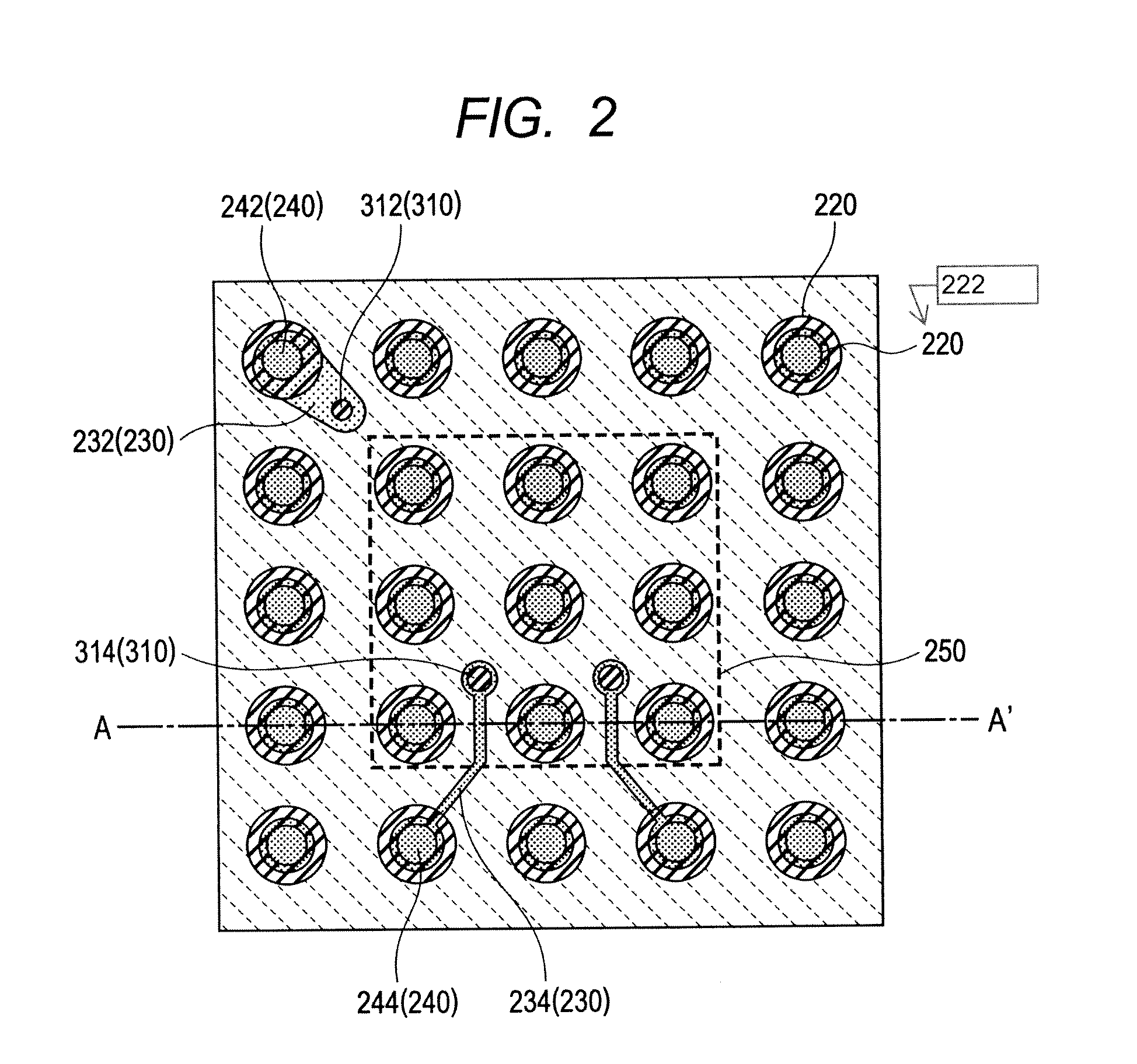
[0032]As shown in FIG. 5, in the interposer 210 a solder resist layer 220 is formed on the interposer 210's surface opposite to the interconnection substrate 10 except the areas of solder resist openings 223 over external coupling terminals 240 and solder resist openings 222. Each solder resist opening 223 lies over an external coupling terminal 240. Each solder resist opening 222 is formed over an interconnect wire 234 between external coupling terminals 240. Each interconnect wire 234 is passed between external coupling terminals 240 arranged along an edge of the semiconductor chip 250.

[0033]Since the semiconductor chip 250 restricts expansion and contraction of the interposer 210, a solder resist crack due to the difference in thermal expansion coefficient tends to occur in an area which overlaps the vicinity of an edge of the semiconductor chip 250. According to the second embodiment, a solder resist opening 222 is provided over an interconnect wire 230 passing between external...


PUM


Abstract

A semiconductor device includes an interposer having a base member including a first surface and a second surface opposite to the first surface, a first interconnect formed on the first surface of the base member, a first insulating film formed on the first surface of the base member, a first external terminal and a second external terminal neighboring the first external terminal formed on the second surface of the base member, a second interconnect formed on the second surface of the base member and passing between the first external terminal and the second external terminal, and a second insulating film formed on the second surface of the base member, a semiconductor chip mounted on the first insulating film, a sealing resin formed on the first insulating film and sealing the semiconductor chip. The second insulating film has an opening so that the second interconnect is exposed in an area.

Description

CROSS-REFERENCE TO RELATED APPLICATION[0001]The present application is a Continuation Application of U.S. patent application Ser. No. 12 / 929,665, filed on Feb. 7, 2011, which is based on and claims priority from Japanese patent application No. 2010-30438, filed on Feb. 15, 2010, the entire contents of which is incorporated herein by reference.BACKGROUND[0002]1. Field of the Invention[0003]The present invention relates to a semiconductor device in which a semiconductor package with an interposer is mounted over an interconnection substrate, a semiconductor package, an interposer, a semiconductor device manufacturing method, and an interposer manufacturing method.[0004]2. Description of Related Art[0005]For example, BGA packages and LGA packages are semiconductor packages. Semiconductor packages are anticipated to provide high reliability, particularly long-term reliability such as temperature cyclicity. If the temperature of a semiconductor device in which a semiconductor package is ...

Claims


Application Information

Patent Timeline
Patent Type & Authority Applications(United States)
IPC IPC(8): H01L23/48
CPCH01L2924/01079H01L23/562H01L2224/16237H01L24/48H05K3/3452H01L23/49838H01L2224/73265H01L2224/32225H01L2224/48227Y10T29/49124H01L2224/48091H01L2224/48228H01L23/49827H01L2924/15311H05K2201/0989H01L24/16H01L2924/15183H01L21/563H01L24/29H05K3/3436H05K2201/10378H01L23/3128H05K1/141H01L2924/00014H01L2924/00H01L2924/3512H01L2924/00012H01L24/73H01L2924/181H01L2224/45099H01L2224/45015H01L2924/207
Inventor SHIBUYA, KOUJIROU
Owner RENESAS ELECTRONICS CORP
Why Eureka
Try Eureka