
Method of forming gate conductor structures

a gate conductor and structure technology, applied in the field of semiconductor processing, can solve the problems of limited capability of conventional lithography to achieve the effect of achieving small features of minimum size, limited resolution and accuracy and limited ability of conventional lithographic processes to print small features. , to achieve the effect of improving line edge roughness (ler) and reducing resist budg

Active Publication Date: 2012-11-15
NAN YA TECH
View PDF3 Cites 3 Cited by
  • Summary
  • Abstract
  • Description
  • Claims
  • Application Information

AI Technical Summary

Benefits of technology

[0007]It is one object of the present invention to provide an improved method of forming fine semiconductor structures such as gate conductor structures with improved line edge roughness (LER) and reduced resist budget.

Problems solved by technology

As known in the art, one limitation to achieving smaller sizes of IC device features is the capability of conventional lithography.
Conventional IC lithographic processes are limited in their ability to print small features, such as contacts, trenches, polysilicon lines or gate conductor structures.
Generally, conventional lithographic processes (e.g., projection lithography and EUV lithography) do not have sufficient resolution and accuracy to consistently fabricate small features of minimum size.
Resolution can be adversely impacted by a number of phenomena including: wavelength of light, diffraction of light, lens aberrations, mechanical stability of the resist, contamination, optical properties of resist, resist contrast, resist swelling, thermal flow of resist, etc.
As such, the critical dimensions of contacts, trenches, gates, and, thus, IC devices, are limited in how small they can be.
Another difficulty arising from the continuing small dimensions involved in the creation of gate conductor structures is the tendency in the lithography process to experience resist erosion, pattern collapse, uncontrolled line edge roughness (LER).
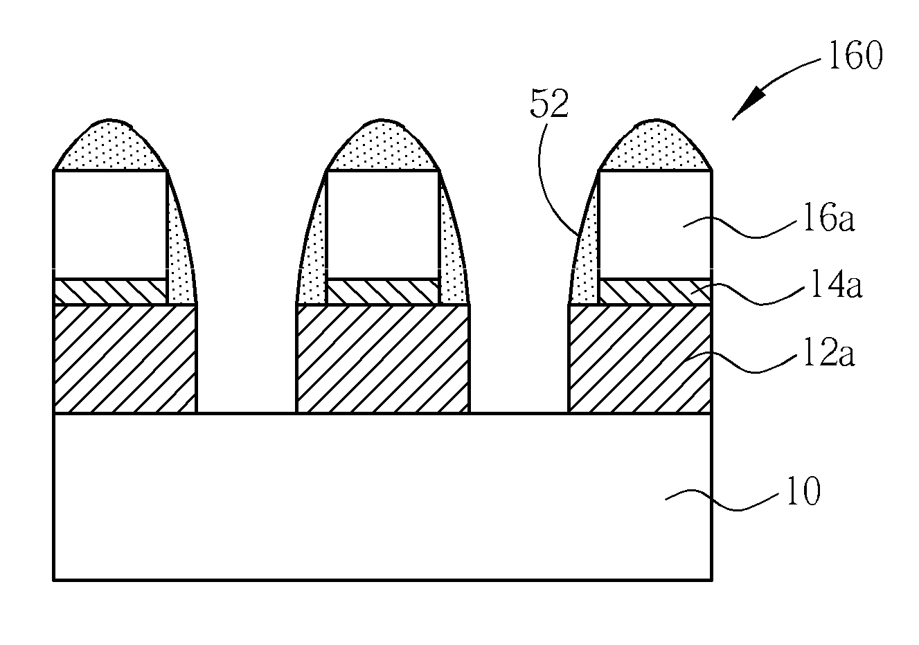
However, severe corner rounding defects are found at the upper portion of the hard mask, which adversely affects the integrity of the gate conductor and results in worsened LER.

Method used


Image

  • Method of forming gate conductor structures
  • Method of forming gate conductor structures
  • Method of forming gate conductor structures

Examples


Embodiment Construction

[0013]In the following detailed description, reference is made to the accompanying drawings, which form a part hereof, and in which is shown by way of illustration specific examples in which the embodiments may be practiced. These embodiments are described in sufficient detail to enable those skilled in the art to practice them, and it is to be understood that other embodiments may be utilized and that structural, logical and electrical changes may be made without departing from the described embodiments. The following detailed description is, therefore, not to be taken in a limiting sense, and the included embodiments are defined by the appended claims.

[0014]The term “horizontal” as used herein is defined as a plane parallel to the conventional major plane or surface of the semiconductor chip or die substrate, regardless of its orientation. The term “vertical” refers to a direction perpendicular to the horizontal as just defined. Terms, such as “on”, “above”, “below”, “bottom”, “to...


PUM

PropertyMeasurementUnit
thicknessaaaaaaaaaa
line edge roughnessaaaaaaaaaa
sizesaaaaaaaaaa

Abstract

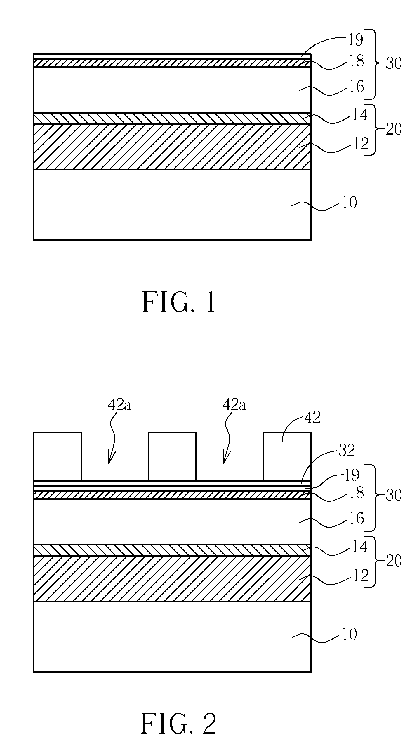
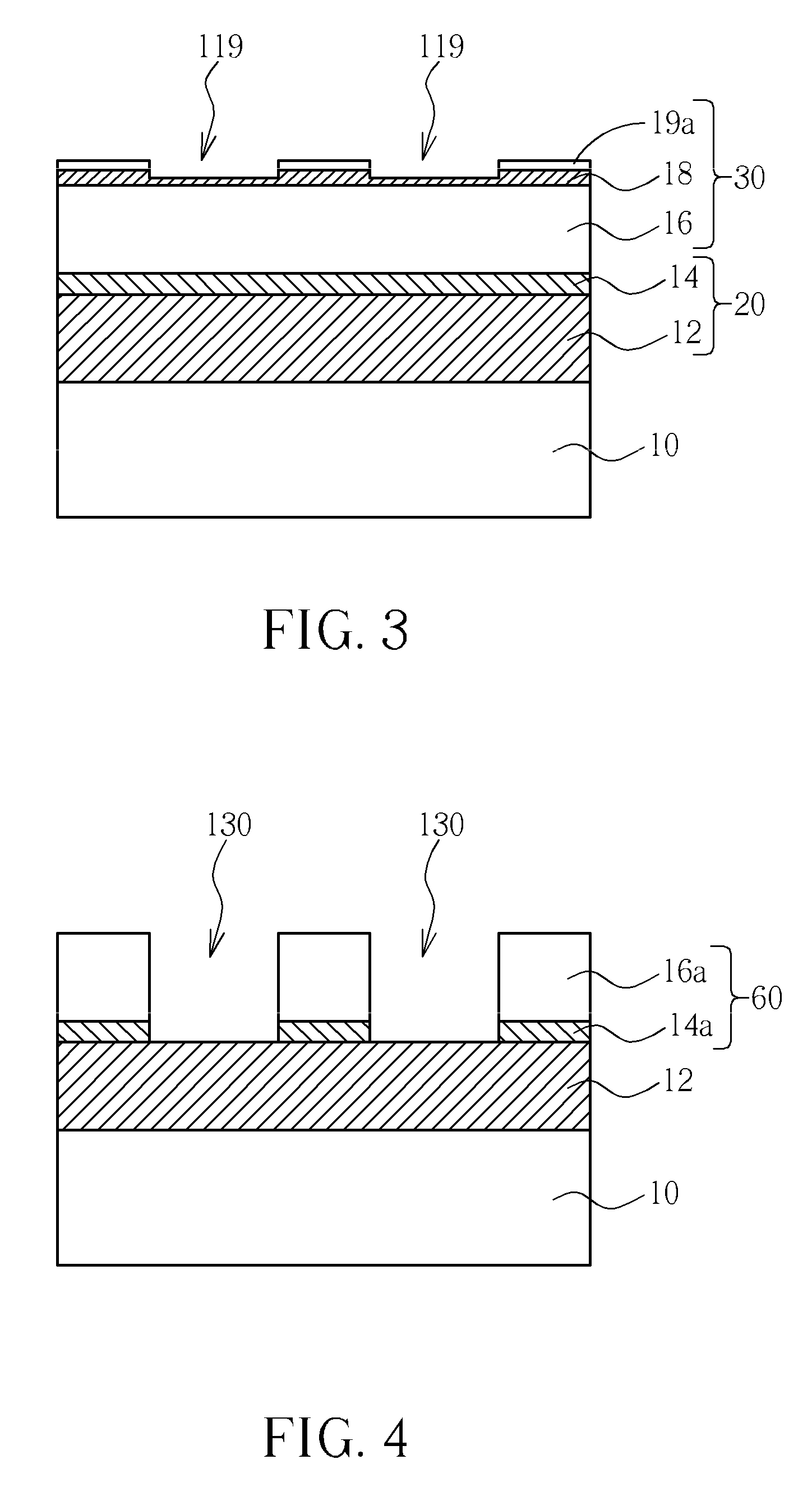
A method of forming gate conductor structures. A substrate having thereon a gate electrode layer is provided. A multi-layer hard mask is formed overlying the gate electrode layer. The multi-layer hard mask comprises a first hard mask, a second hard mask, and a third hard mask. A photoresist pattern is formed on the multi-layer hard mask. A first etching process is performed to etch the third hard mask, using the photoresist pattern as a first etch resist, thereby forming a patterned third hard mask. A second etching process is performed to etch the second hard mask and the first hard mask, using the patterned third hard mask as a second etch resist, thereby forming a patterned first hard mask. A third etching process is performed to etch a layer of the gate electrode layer, using the patterned first hard mask as a third etch resist.

Description

BACKGROUND OF THE INVENTION[0001]1. Field of the Invention[0002]The present invention relates generally to the semiconductor processing. More particularly, the present invention relates to a method of forming gate conductor structures with improved line edge roughness (LER) and reduced resist budget.[0003]2. Description of the Prior Art[0004]As known in the art, one limitation to achieving smaller sizes of IC device features is the capability of conventional lithography. Lithography is the process by which a pattern or image is transferred from one medium to another. Conventional IC lithography uses ultra-violet (UV) sensitive photoresist. UV light is projected to the photoresist through a reticle or mask to create device patterns on an IC. Conventional IC lithographic processes are limited in their ability to print small features, such as contacts, trenches, polysilicon lines or gate conductor structures.[0005]Generally, conventional lithographic processes (e.g., projection lithogr...

Claims


Application Information

Patent Timeline
Patent Type & Authority Applications(United States)
IPC IPC(8): G03F7/20
CPCH01L21/28123H01L21/32139H01L21/28132
Inventor WU, CHANG-MINGCHEN, YI-NANLIU, HSIEN-WEN
Owner NAN YA TECH
Learn More