
Glass Wafers for Semiconductor Fabrication Processes and Methods of Making Same

a technology of glass wafers and semiconductors, applied in the field of glass wafers, to achieve the effect of improving the functionality of gripping the wafer

Active Publication Date: 2012-11-01
CORNING INC
View PDF5 Cites 28 Cited by
  • Summary
  • Abstract
  • Description
  • Claims
  • Application Information

AI Technical Summary

Benefits of technology

The patent text describes the use of glass wafers in semiconductor fabrication processes and the importance of the glass's coefficient of thermal expansion (CTE) being equal to that of silicon semiconductor wafers. The problem addressed in the patent is finding a way to apply a layer or film to the glass wafer that matches the CTE of the final silicon composite, without adding significant cost or complexity to the process. The solution proposed is to use a layer or film that can be applied without vacuum deposition and that has desirable attributes such as activating optical sensors or improving the function of gripping tools. The patent also describes the use of standard photoresist films or photoresist containing carbon particles to change the dielectric properties of the glass wafer.

Problems solved by technology

However, one problem with using glass is that many of the sensors are designed to sense silicon semiconductor wafers.

Method used


Image

  • Glass Wafers for Semiconductor Fabrication Processes and Methods of Making Same
  • Glass Wafers for Semiconductor Fabrication Processes and Methods of Making Same
  • Glass Wafers for Semiconductor Fabrication Processes and Methods of Making Same

Examples


Embodiment Construction

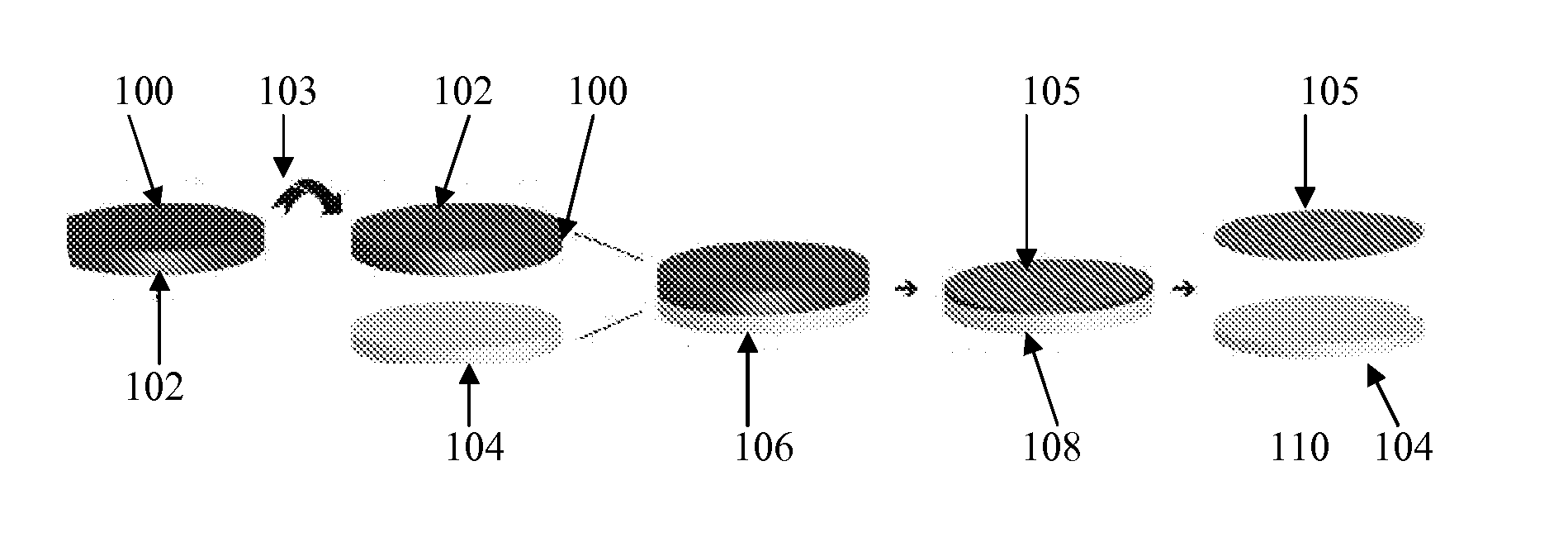
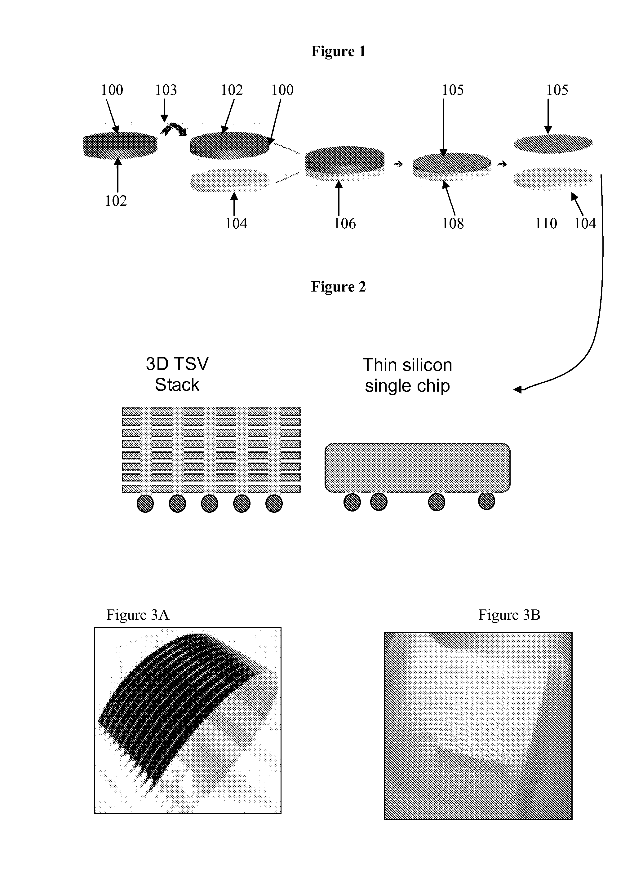
[0025]Herein, the formation of a circuit or an integrated circuit is used as an example of the use of glass carrier wafers in lithographic processes. In addition to circuitry or integrated circuits, the teachings herein are applicable to processes that can be used to produce other devices, including MEMS, LED, CIS, c-PV, memory, Logic ICs, RF / Analog ICs, microfluidic devices, microdisplays, Laser / VCSEL, fuel cells, microbatteries, power devices, and the like. For convenience, the term “coating” is intended to include films, coatings, or layers disposed on a surface. Generally, the coatings will involve an opaque coating that blocks light used in fabrication tool sensors, which ranges from the infrared to the visible to the ultraviolet (about 1300 nm to about 350 nm), or a transparent coating to change the dielectric properties of the wafer so that the wafer can be used with electrostatic chucks (e.g., a SnO2 coating for changing dielectric properties of the wafer).

[0026]The initial ...


PUM

PropertyMeasurementUnit
distanceaaaaaaaaaa
temperatureaaaaaaaaaa

Abstract

The present disclosure is directed to the use of glass wafers as carriers, interposers, or in other selected applications in which electronic circuitry or operative elements, such as transistors, are formed in the creation of electronic devices. The glass wafers generally include a glass having a coefficient of thermal expansion equal to or substantially equal to a coefficient of thermal expansion of semiconductor silicon, an indexing feature, and a coating on at least a portion of one face of the glass.

Description

CROSS-REFERENCE TO RELATED APPLICATION[0001]This application claims the benefit of priority under 35 USC 119 of U.S. Provisional Patent Application Ser. No. 61 / 410,599 filed on Nov. 5, 2010 the content of which is relied upon and incorporated herein by reference in its entirety.TECHNICAL FIELD[0002]The disclosure is directed to glass wafers that can be used as a replacement for silicon wafers in semiconductor fabrication processes, including in the automated equipment used to produce integrated circuits and electronic elements.BACKGROUND[0003]There is a growing need for less expensive methods of processing silicon wafers to make integrated circuits (ICs), MEMS devices, logic ICs, power devices, and other elements used in modern electronics. At the present time, silicon wafers are used not only for the active integrated circuitry and other circuit elements, but are also used as carriers, interposers, and mechanical elements that do not contain circuitry or other features used in elec...

Claims


Application Information

Patent Timeline
Patent Type & Authority Applications(United States)
IPC IPC(8): H01L23/15B32B17/06H01L21/50
CPCC03C17/00H01L21/02422H01L21/02444H01L21/02491H01L21/0245H01L21/02488H01L2224/16145H01L21/50
Inventor CANALE, JOSEPH EUGENEKING, JEFFREY STAPLETONTROTT, GARY RICHARD
Owner CORNING INC
Learn More