
FIB Process for Selective and Clean Etching of Copper

a selective and clean etching technology, applied in vacuum evaporation coatings, sputtering coatings, coatings, etc., can solve the problems of difficult to achieve clean uniform fib etching of copper for ce, uneven fib etching of copper, and rough surface of etched copper, etc., to prevent electrical short circuit, high stickiness and long residence time

Inactive Publication Date: 2012-08-23
TIZA LAB
View PDF4 Cites 5 Cited by
  • Summary
  • Abstract
  • Description
  • Claims
  • Application Information

AI Technical Summary

Benefits of technology

These agents effectively protect dielectrics and oxidize re-deposited copper, ensuring complete electrical disconnection and preventing electrical short circuits, while maintaining the integrity of the dielectric surface during copper etching in FIB processes.

Problems solved by technology

Achieving clean uniform FIB etching of copper for CE is difficult.
In spite of significant past efforts to improve the quality of FIB copper etching processes, problems persist and improvements are needed in two main areas.
Both of these problems arise from the properties of copper.
This can inevitably lead to the unwanted re-deposition of conductive copper which causes problems as discussed below.
Grains with different orientations exhibit significantly different FIB etching rates and, therefore, FIB etching of copper is very non-uniform and uneven.
It results in a very rough surface on the etched copper, and may perforate the copper layer down to the underlying dielectric.
This may lead to significant damage of the underlying dielectric, and may result in electrical short circuiting of IC circuits from re-deposited electrically conductive copper.
Past efforts to improving selectivity have focused principally on protecting the dielectric rather than enhancing the removal of copper, because the required selectivity that is achievable for copper etching is low relative to other materials, e.g., aluminum, where volatile etching byproducts are created.
Further, the ion beam sputtering process causes copper re-deposition all about the area exposed by the ion beam.
This creates significant problems since the milled copper material that is intended to be removed re-deposits in this area, making electrical isolation of a signal difficult or impossible.
However, not all oxidizing agents will work with copper.
Halogens, with the exception of fluorine, spontaneously react with and corrode copper without any activation by an ion beam, and they seriously degrade the conductivity of the copper.
Even if halogen agents such as chlorine, bromine and iodine are carefully controlled, they can remain in the FIB vacuum chamber for a long time and continue to corrode any exposed copper.
Otherwise, subsequent operations can be seriously affected.
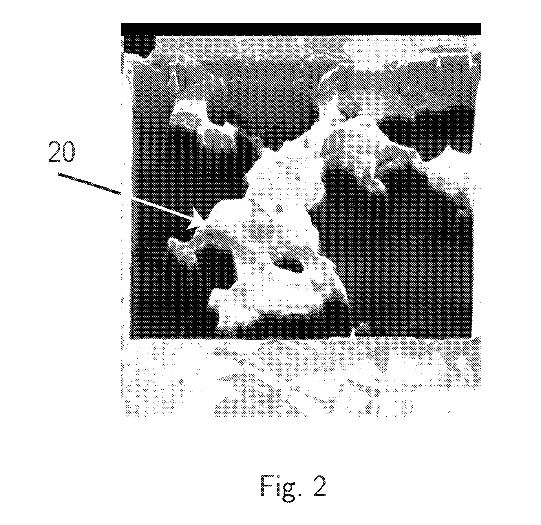
As shown, the underlying dielectric is heavily damaged in areas where the copper removal was the greatest, while in other areas significant amounts of copper remain to be removed.
This means that it is necessary to expose the copper to the ion beam for a longer period of time, and because of the unevenness of copper removal the ion beam may inadvertently damage some spots of the underlying dielectric.
However, these compounds have been found to be useless for protecting the new low-k dielectrics being increasingly used in ICs.
The main problem is that many low-k dielectrics contain carbon as one of the main components of the dielectric structure, which is why low-k dielectrics are sometimes called “organic” dielectrics.
While Nitro-ethanol has been effective in limiting dielectric etching, it has not been very effective addressing the problem of re-deposition of sputtered conductive copper material on surfaces adjacent to the IC work area.
This re-deposited material may render the IC partially or totally inoperative by electrically short circuiting interconnects or grounding copper power planes.
From the figure, it can be concluded that while the Nitro-ethanol copper etch assisting compound functions well to protect the underlying dielectric, it is not effective in addressing conductive copper re-deposition.

Method used


Image

  • FIB Process for Selective and Clean Etching of Copper
  • FIB Process for Selective and Clean Etching of Copper
  • FIB Process for Selective and Clean Etching of Copper

Examples


Embodiment Construction

[0026]The invention is particularly well adapted to the focused ion beam (FIB) etching of copper interconnects, power and ground planes and the like in ICs for circuit editing (CE), and will be described in that context. However it will be appreciated that this is illustrative of only one utility of the invention, and that the invention has greater applicability.

[0027]Conventional FIB apparatus and operations are well known and will not be described in detail herein. U.S. Pat. No. 7,060,196, which is hereby incorporated by reference herein, discloses FIB apparatus that uses Gallium (Ga+) ions for milling copper over organic dielectrics in a context and environment similar to that of the present invention, and such FIB apparatus may be used to practice the invention.

[0028]Although conventional FIB apparatus and processes have typically employed Gallium (Ga+) ions, different metal ions, non-metal ions, noble gas ions and molecular ions may also be used advantageously in FIB processes....


PUM

PropertyMeasurementUnit
boiling pointsaaaaaaaaaa
temperatureaaaaaaaaaa

Abstract

Etch assisting agents for focused ion beam (FIB) etching of copper for circuit editing of integrated circuits both prevent loss of adjacent dielectric due to sputtering by the ion beam, and render sputtered re-deposited copper on adjacent surfaces non-conductive to avoid electrical short circuits. The agents are characterized by having an N—N (N being Nitrogen) bonding in their molecules and boiling points between about 70° C. and about 220° C., and include hydrazine and water solutions, hydrazine derivatives, NitrosAmine derivatives saturated with two hydrocarbon groups selected from Methyl, Ethyl, Propyl and Butyl, NitrosAmine related compounds, and Nitrogen Tetroxide. Preferred agents are Hydrazine monohydrate (HMH), HydroxyEthylHydrazine (HEH), CEH, BocMH, BocMEH, NDMA, NDEA, NMEA, NMPA, NEPA, NDPA, NMBA, NEBA, NPYR, NPIP, NMOR and Carmustine, alone or in combination with Nitrogen Tetroxide. The agents are effective for etching copper in high aspect ratio (deep) holes.

Description

FIELD OF THE INVENTION[0001]This invention relates generally to focused ion beam etching of copper and copper materials, and more particularly to the chemically-assisted etching of copper over dielectric materials.BACKGROUND[0002]Copper (Cu) is the primary material used in integrated circuits (ICs) to create electrically conductive interconnects, and the etching of copper in ICs using focused ion beam (FIB) techniques is important in the field of circuit editing (CE) for failure verification and debugging of the ICs. Circuit editing of ICs with a focused-ion-beam (FIB) system requires that copper planes and traces be milled (cut) uniformly and cleanly so as to electrically isolate circuit elements across the separation created.[0003]Achieving clean uniform FIB etching of copper for CE is difficult. In spite of significant past efforts to improve the quality of FIB copper etching processes, problems persist and improvements are needed in two main areas. These two areas are reducing e...

Claims


Application Information

Patent Timeline
Patent Type & Authority Applications(United States)
IPC IPC(8): C23F4/00
CPCC23F4/00H01L21/76892H01L21/32136H01L21/00
Inventor MAKAROV, VLADIMIR V.
Owner TIZA LAB
Learn More