
Multi-nary group ib and via based semiconductor

a semiconductor and semiconductor technology, applied in the field of multi-nary semiconductor materials, can solve the problems of difficult cost effective creation of solar cells with higher conversion efficiency, time-consuming one-step fabrication process, and increased risk of material migration and/or phase separation during fabrication, so as to achieve high open-circuit voltage solar cells, low cost, and high efficiencies

Inactive Publication Date: 2012-07-05
AERIS CAPITAL SUSTAINABLE IP
View PDF2 Cites 42 Cited by
  • Summary
  • Abstract
  • Description
  • Claims
  • Application Information

AI Technical Summary

Benefits of technology

[0008]For many of the embodiments herein, it is also possible to have two or more elements of IB elements in the chalcogenide particle and / or the resulting intermediate film and / or final absorber layer. The present embodiments further enhance performance by including at least two or more group VIA elements to form a senary or higher multi-nary IBIIIAVIA alloy. Some embodiment may relate to senary or higher semiconductors containing at least two IB elements, two VIA elements, and at least two other elements from the groups consisting of IIB, IIIA, and IVA.
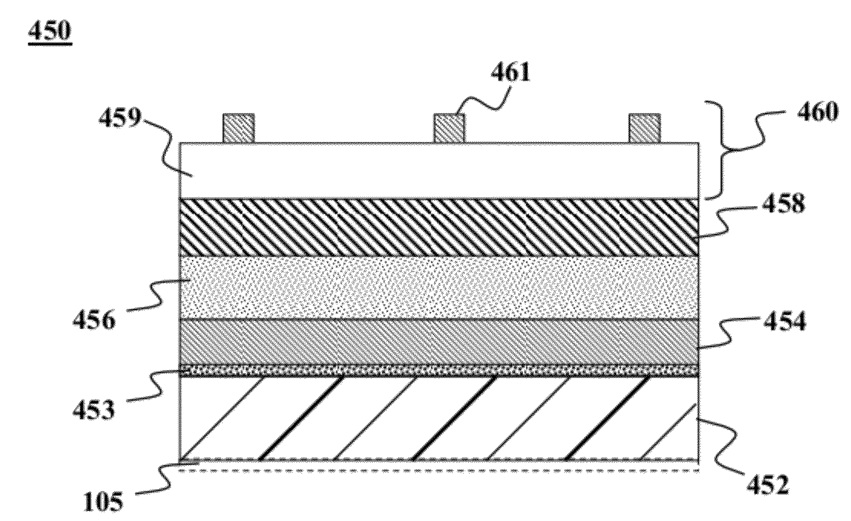
[0014]In another embodiment of the present invention, an optoelectronic device is provided a (Ag,Cu)(In,Ga)(SeS)2 absorber layer having a surface region, a bulk region and a transition region between the surface region and the bulk region, wherein a surface region S / (S+Se) molar ratio in the surface region is greater than a surface region Ag / (Ag+Cu) ratio in the surface region and provides an increased sulfur interface for junction partner formation. Without being bound to any particular theory, the junction partner layer used with the thin film absorber layer may be CdS and the sulfur interface on the thin film absorber may improve junction partner formation or growth.
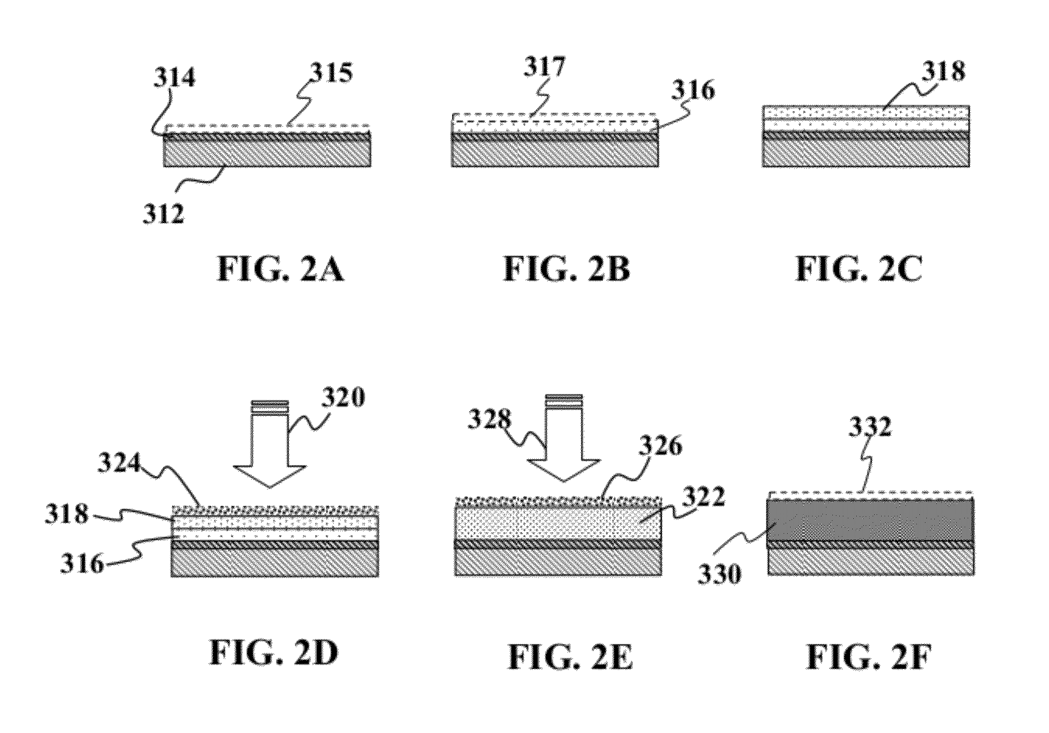
[0028]One notable problem encountered when creating CIG(S)Se films for solar cells using low cost 2-step selenization methods is preventing Ga from segregating to the back of the film. Two-step selenization methods entail one step where a metal, oxide, or chalcogenide (or other Ag, Au, Cu, In, Ga, S, or Se containing compounds) precursor film is deposited, and then subsequently selenized (and / or sulfidized) in a second step. The approach described herein is to create (Ag,Cu)(In,Ga)(Se,S)2 (hereafter referred to as ACIGSS) by adding Ag to the precursor film. It has been found that this enables more of the Ga to remain forward in the film. Ga at the front surface of the film allows for higher open-circuit voltage solar cells and therefore higher efficiencies.

Problems solved by technology

These electronic devices have been traditionally fabricated using silicon (Si) as a light-absorbing, semiconducting material in a relatively expensive production process.
Although material content through the depth of the layer is more controllable, this one step type fabrication process is typically a time consuming process.
By contrast, multi-step fabrication techniques which involve deposition and then a subsequent anneal in one or more steps in a group VIA or other reactive environment can sometimes be a higher throughput process that, unfortunately, is more susceptible to migration and / or phase separation of material during fabrication.
One problem faced with thin-film type solar cells is the difficulty in cost effectively creating solar cells with higher conversion efficiencies, more on par with the efficiencies of their crystalline silicon counterparts.

Method used


Image

  • Multi-nary group ib and via based semiconductor
  • Multi-nary group ib and via based semiconductor
  • Multi-nary group ib and via based semiconductor

Examples


embodiment 1

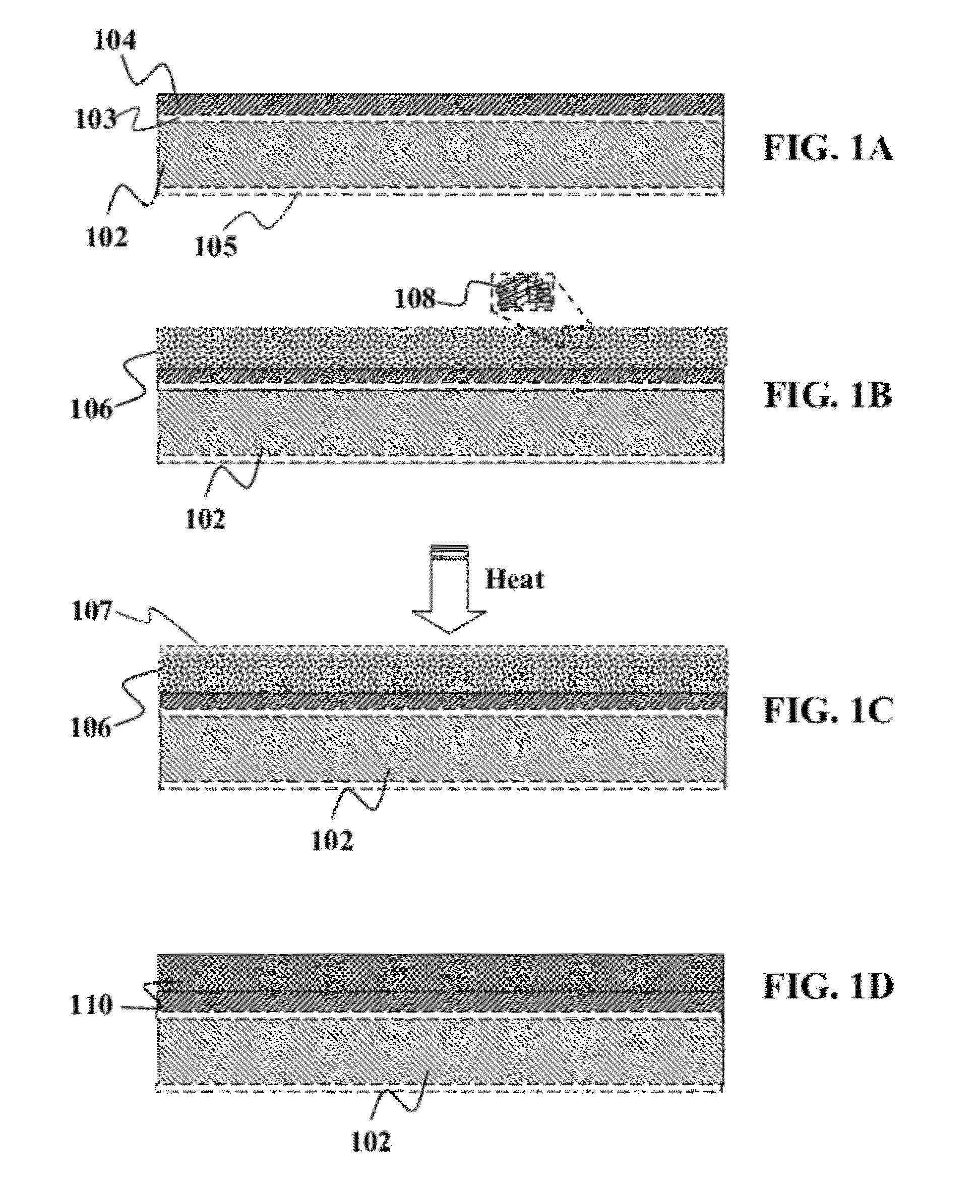
[0082]A metal foil substrate was sputtered with Mo to form a 500 nm to 1000 nm Mo film to serve as the back contact. A barrier layer of 50 nm to 300 nm of Chromium, TiN, HfN, or other transition metal nitride barrier was formed onto the Mo back contact. A precursor ink comprised of Cu, In, Ga, and Ag, and atomic ratios Ag / (Ag+Cu)=0.1-0.3, Ga / (Ga+In)=0.35-0.5, and (Ag+Cu) / (Ga+In)=0.80-1.0. For the present embodiment, an approximately 0.5-2.5 micron thick layer of the precursor material containing solution is deposited on the substrate. The precursor material may be dispersed in a solvent such as water, alcohol or ethylene glycol with the aid of organic surfactants and / or dispersing agents described herein to form an ink.

[0083]The precursor layer is annealed with a ramp-rate of 1-5° C. / sec, optionally over 5° C. / sec, to a temperature of about 225° to about 575° C. optionally for about 30 seconds to about 600 seconds to enhance densification and / or alloying between Ag, Cu, In, and Ga i...

embodiment 2

[0087]A metal foil substrate was sputtered with Mo to form a 500 nm to 1000 nm Mo film to serve as the back contact. A barrier layer of 50 nm to 300 nm of Chromium, TiN, HfN, or other transition metal nitride barrier was formed onto the Mo back contact. A precursor ink comprised of Cu, In, Ga, and Ag, and atomic ratios Ag / (Ag+Cu)=0.2-0.3, Ga / (Ga+In)=0.3-0.4, and (Ag+Cu) / (Ga+In)=0.8-0.9. For the present embodiment, an approximately 0.5-2.5 micron thick layer of the precursor material containing solution is deposited on the substrate. The precursor material may be dispersed in a solvent such as water, alcohol or ethylene glycol with the aid of organic surfactants and / or dispersing agents described herein to form an ink.

[0088]The precursor layer is annealed with a ramp-rate of 1-5° C. / sec, optionally over 5° C. / sec, to a temperature of about 225° to about 575° C. optionally for about 30 seconds to about 600 seconds to enhance densification and / or alloying between Ag, Cu, In, and Ga in ...

embodiment 3

[0092]A metal foil substrate was sputtered with Mo to form a 500 nm to 1000 nm Mo film to serve as the back contact. A barrier layer of 50 nm to 300 nm of Chromium, TiN, HfN, or other transition metal nitride barrier was formed onto the Mo back contact. The method may be used to form a IB-IIB-IVA-VIA absorber material. A precursor ink is provided wherein Ag / IB=0.1-0.4. A method of forming (Ag,Cu)xZnySn2SaSeb (ACZTSSe) layers with well-defined total bulk stoichiometries, wherein x ranges from 1.5 to 2.5, y ranges from 0.9 to 1.5, z ranges from 0.5 to 1.1, a ranges from 0 to 4.2, optionally from 0.1 to 4.2, and b ranges from 0 to 4.2, optionally from 0.1 to 4.2, and which method is easy to apply and suitable for large scale production of thin film solar cells.

[0093]In one embodiment, the stoichiometric ratio for a ACZTS solar cell precursor foil may be (Ag: 10 at.-%, Cu: 40 at.-%, Zn: 25 at.-%, Sn: 25 at.-%) Optionally, a further object of the invention is to provide a thin film of AC...


PUM

PropertyMeasurementUnit
thicknessaaaaaaaaaa
molar ratioaaaaaaaaaa

Abstract

Methods and devices are provided for forming multi-nary semiconductor. In one embodiment, a method is provided comprising of depositing a precursor material onto a substrate, wherein the precursor material may include or may be used with an additive to minimize concentration of group IIIA material such as Ga in the back portion of the final semiconductor layer. The additive may be a non-copper Group IB additive in elemental or alloy form. Some embodiments may use both selenium and sulfur, forming a senary or higher semiconductor alloy.

Description

CROSS-REFERENCE TO RELATED APPLICATIONS[0001]This application claims priority to U.S. Provisional Application Ser. Nos. 61 / 430,131 filed 5 Jan. 2011, 61 / 502,853 filed 29 Jun. 2011, and 61 / 505,084 filed 6 Jul. 2011. All applications are fully incorporated herein by reference for all purposes.FIELD OF THE INVENTION[0002]This invention relates generally to multi-nary semiconductor materials, more specifically to senary or higher semiconductors suitable but not limited to use in optoelectronic devices.BACKGROUND OF THE INVENTION[0003]Solar cells and solar modules convert sunlight into electricity. These electronic devices have been traditionally fabricated using silicon (Si) as a light-absorbing, semiconducting material in a relatively expensive production process. To make solar cells more economically viable, solar cell device architectures have been developed that can inexpensively make use of thin-film, preferably non-silicon, light-absorbing semiconductor materials such as but not l...

Claims


Application Information

Patent Timeline
Patent Type & Authority Applications(United States)
IPC IPC(8): H01L29/26
CPCH01L21/268H01L29/263H01L31/022466H01L31/0749Y02E10/541H01L31/0322H01L31/03923H01L31/03928Y02P70/50
Inventor JACKREL, DAVID B.DICKEY, KATHERINEPOLLOCK, KRISTINWOODRUFF, JACOBSTONE, PETERBROWN, GREGORY
Owner AERIS CAPITAL SUSTAINABLE IP
Learn More