Chemical-mechanical planarization method and method for fabricating metal gate in gate-last process
a technology of metal gate and gate-last, which is applied in the direction of basic electric elements, electrical equipment, and semiconductor devices, can solve the problems of short circuit in the device, limit the tuning range of metal gate cmp process, etc., and achieve the effect of improving the uniformity of the inner die and preventing short circuits in the devi
- Summary
- Abstract
- Description
- Claims
- Application Information
AI Technical Summary
Benefits of technology
Problems solved by technology
Method used
Image
Examples
embodiment 1
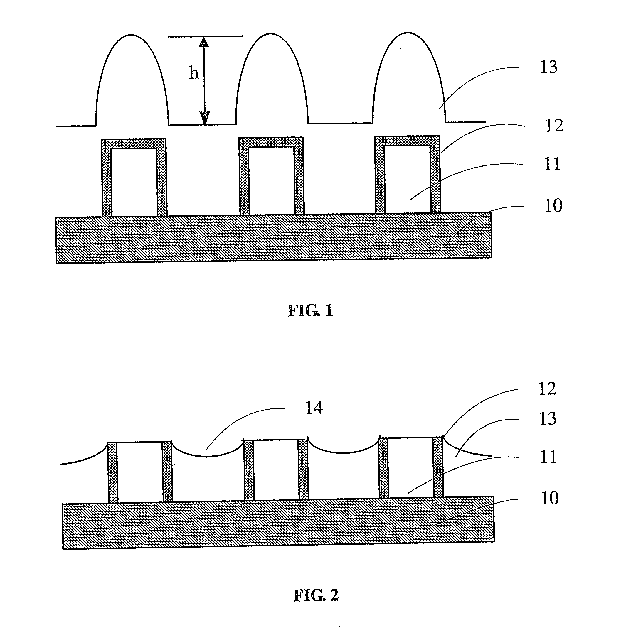
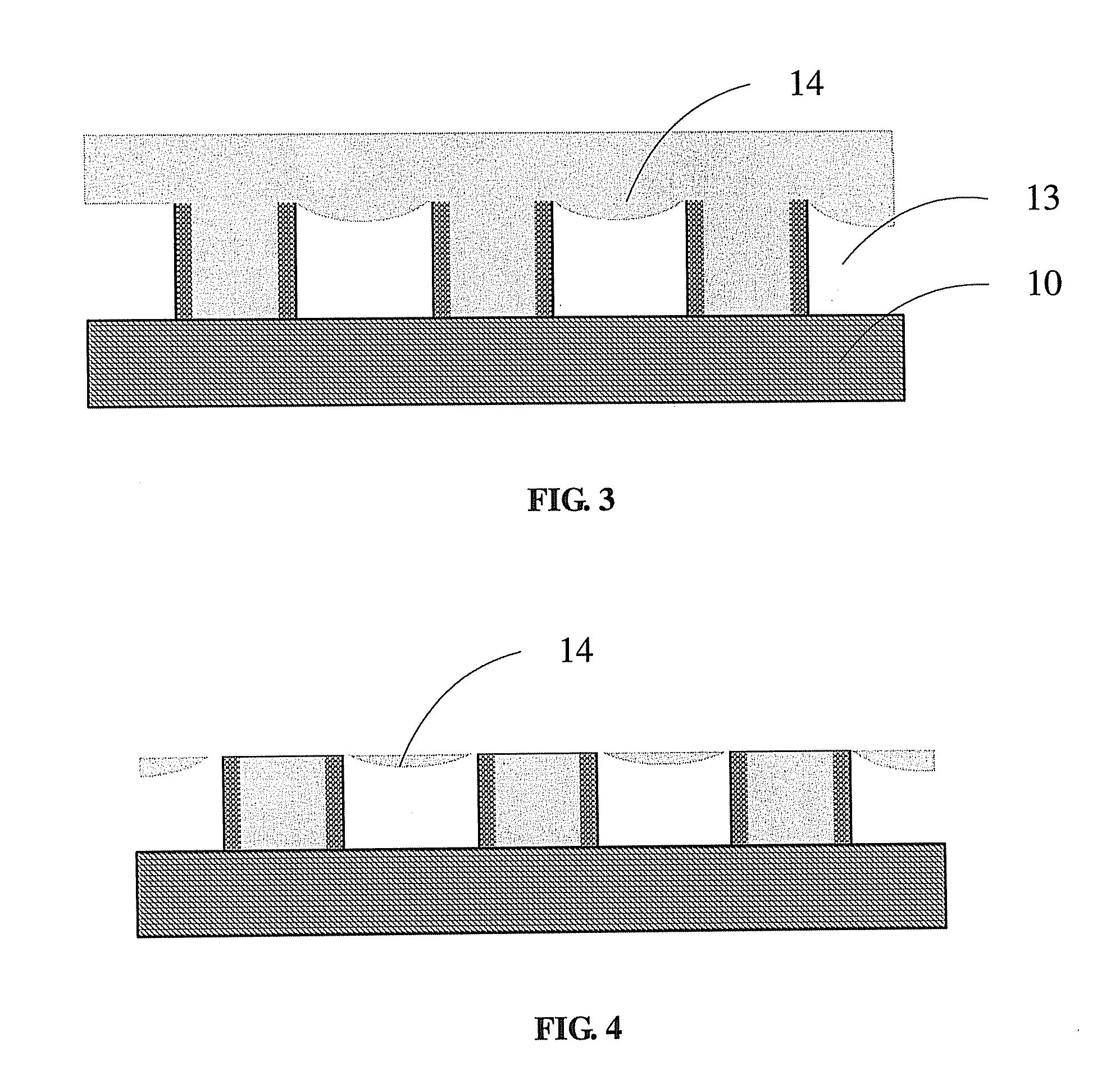
[0044]FIG. 5 illustrates a flow chart of a CMP method according to the embodiment; and FIG. 6—FIG. 8 illustrate the CMP method according to the embodiment.
[0045]As shown in the figures, the method includes:
[0046]Step S1: as shown in FIG. 6, a substrate 100 is provided, including a gate 101 and source / drain regions (not shown) on the sides of the gate 101, the gate 101 and the source / drain regions are overlay by an insulating layer 102, and the insulating layer 102 includes a protruding part 102a above the gate and a recessed part 102b above the surface of the substrate between the gates 101.
[0047]Step S2: selective doping is performed on the insulating layer 102, such that only the protruding part 102a is doped. Preferably, in this embodiment, the selective doping is ion implantation; and a mask layer 103 covers the recessed part 102b of the insulating layer 102, with only the protruding part 102a exposed, and the protruding part 102a is doped through ion implantation in the directi...
embodiment 2
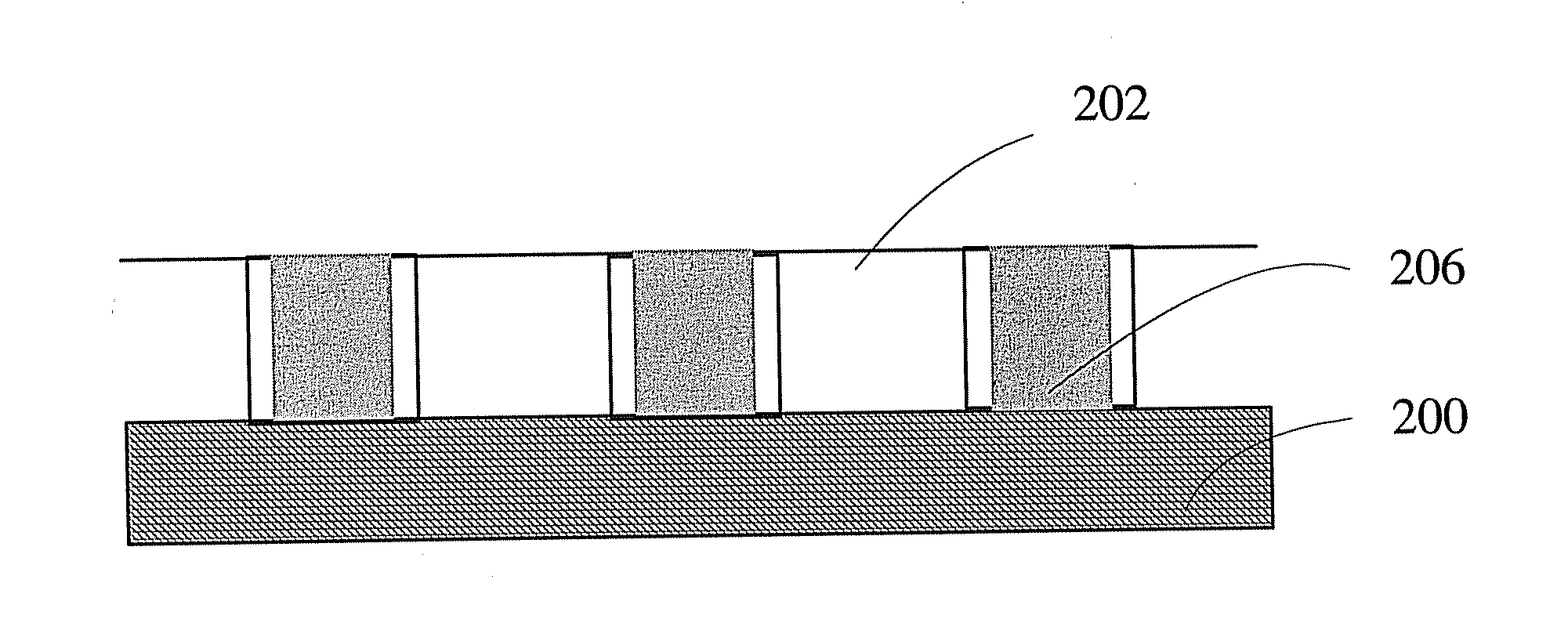
[0054]As an example, a gate-last method for fabricating a typical 32 nm metal gate is described, to show another embodiment of the CMP method. FIG. 9—FIG. 16 illustrate a method for fabricating a metal gate in gate last process according to the embodiment.
[0055]As shown in FIG. 9, a substrate 200 is provided, the substrate 200 includes a dummy gate 201, a gate oxide layer (not shown) and source / drain regions (not shown) on the sides of the dummy gate 200, and the dummy gate 201 and the source / drain regions are overlay by a first insulating layer 208 and a second insulating layer 202.
[0056]Specifically, the substrate 200 may be formed of an elemental semiconductor, e.g., monocrystalline, polycrystalline or amorphous silicon, or monocrystalline, polycrystalline or amorphous silicon-germanium (SiGe); or a compound semiconductor, e.g., silicon carbide (SiC), indium antimonide (InSb), lead telluride (PbTe), indium arsenide (InAs), indium phosphide (InP), gallium arsenide (GaAs), or galli...
PUM
 Abstract
Description
Claims
Application Information
 - R&D
- Intellectual Property
- Life Sciences
- Materials
- Tech Scout
- Unparalleled Data Quality
- Higher Quality Content
- 60% Fewer Hallucinations
Browse by: Latest US Patents, China's latest patents, Technical Efficacy Thesaurus, Application Domain, Technology Topic, Popular Technical Reports.
© 2025 PatSnap. All rights reserved.Legal|Privacy policy|Modern Slavery Act Transparency Statement|Sitemap|About US| Contact US: help@patsnap.com


