
Dicing die bond film

a die-cutting and bonding technology, applied in the direction of heat-activated film/foil adhesives, film/foil adhesives, transportation and packaging, etc., can solve the problem of the circuit on the semiconductor chip being broken, and achieve good tackiness and workability

Inactive Publication Date: 2012-03-15
NITTO DENKO CORP
View PDF32 Cites 44 Cited by
  • Summary
  • Abstract
  • Description
  • Claims
  • Application Information

AI Technical Summary

Benefits of technology

[0010]According to the above-described configuration, because the volume resistivity of the thermosetting type die bond film is 1×10⁻³ Ω·cm or less, a high antistatic effect can be exhibited. Therefore, breakage of the semiconductor chip due to peeling electrification during pickup can be prevented, and electrification when the semiconductor chip with a die bond film is laminated on an adherend can be prevented. As a result, reliability as a device can be improved.
[0011]Because the tensile storage modulus of the thermosetting type die bond film at −20° C. before thermal curing is 10 GPa or less, good tackiness to the adherend and good workability can be obtained. Because the tensile storage modulus is 0.1 GPa or more and relatively high, stress can be easily transferred during expansion.
[0013]In the above-described configuration, the conductive particles are two kinds or more of conductive particles having different average particle sizes, and each kind of the conductive particles preferably has an average particle size of 0.01 μm or more and 10 μm or less. By making the average particle size of the conductive particles 0.01 μm or more, wettability to the adherend can be secured and good tackiness can be exhibited. By making the average particle size of the conductive particles 10 μm or less, a better improvement effect on electrical conductivity and thermal conductivity due to the addition of the conductive particles can be obtained. Further, the thickness of the thermosetting type die bond film can be reduced, high integration can be made possible, and generation of a chip crack caused by projection of the conductive particles from the thermosetting type die bond film can be prevented. Further, by using two kinds of more of the conductive particles having different average particle sizes, the filling factor can be easily improved.
[0014]In the above-described configuration, the content of the conductive particles is preferably 20 to 90 parts by weight relative to 100 parts by weight of an organic component of the thermosetting type die bond film. By making the content of the conductive particles 20 parts by weight or more, a decrease of the conductive function caused by a high volume resistivity due to the formation of a conductive path can be suppressed. By making the content of the conductive particles 90 parts by weight or less, good toughness of the thermosetting type die bond film can be kept and generation of cracks and chipping during handling of the thermosetting type die bond film can be prevented.
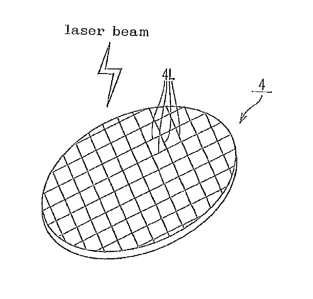
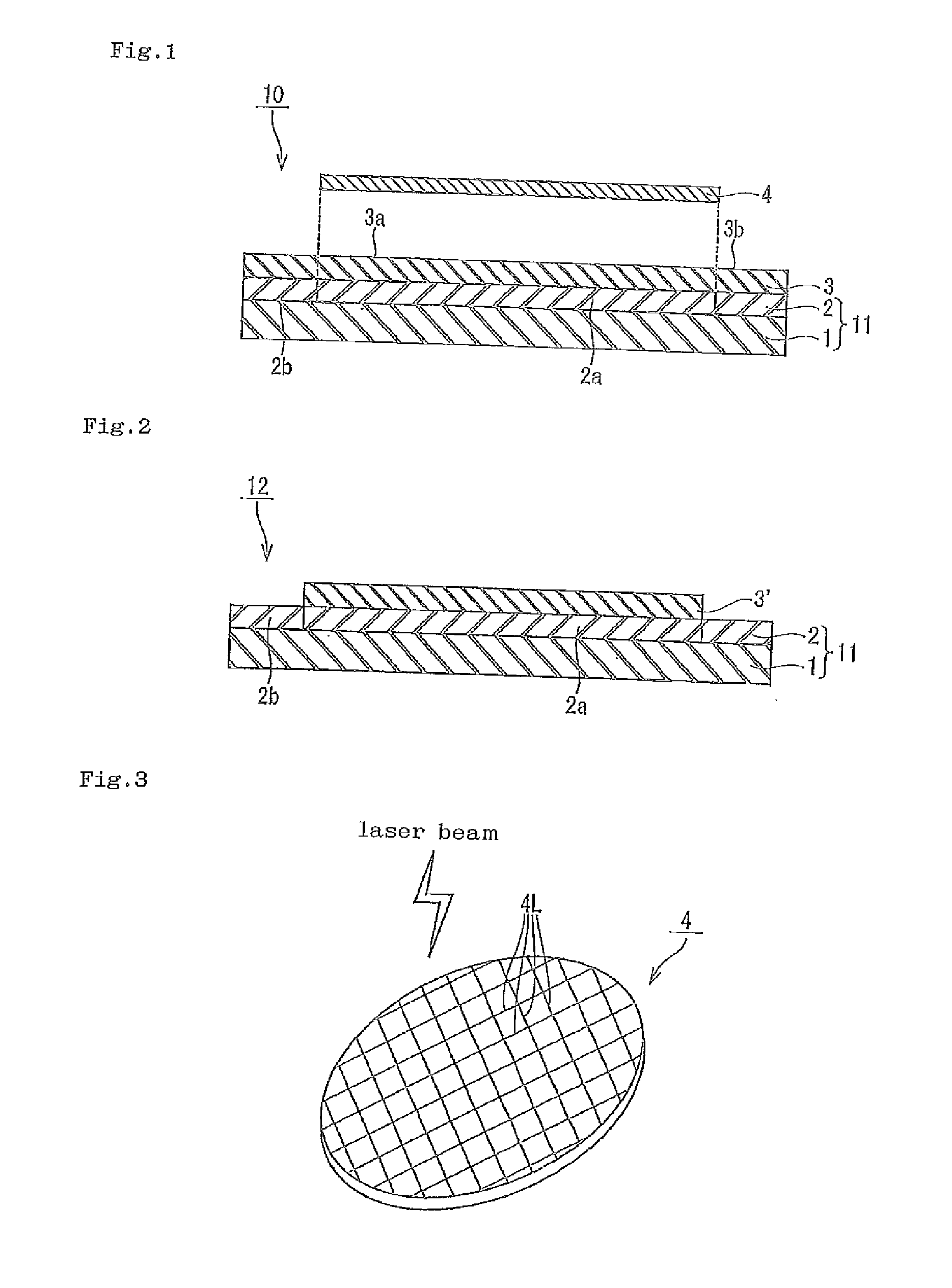
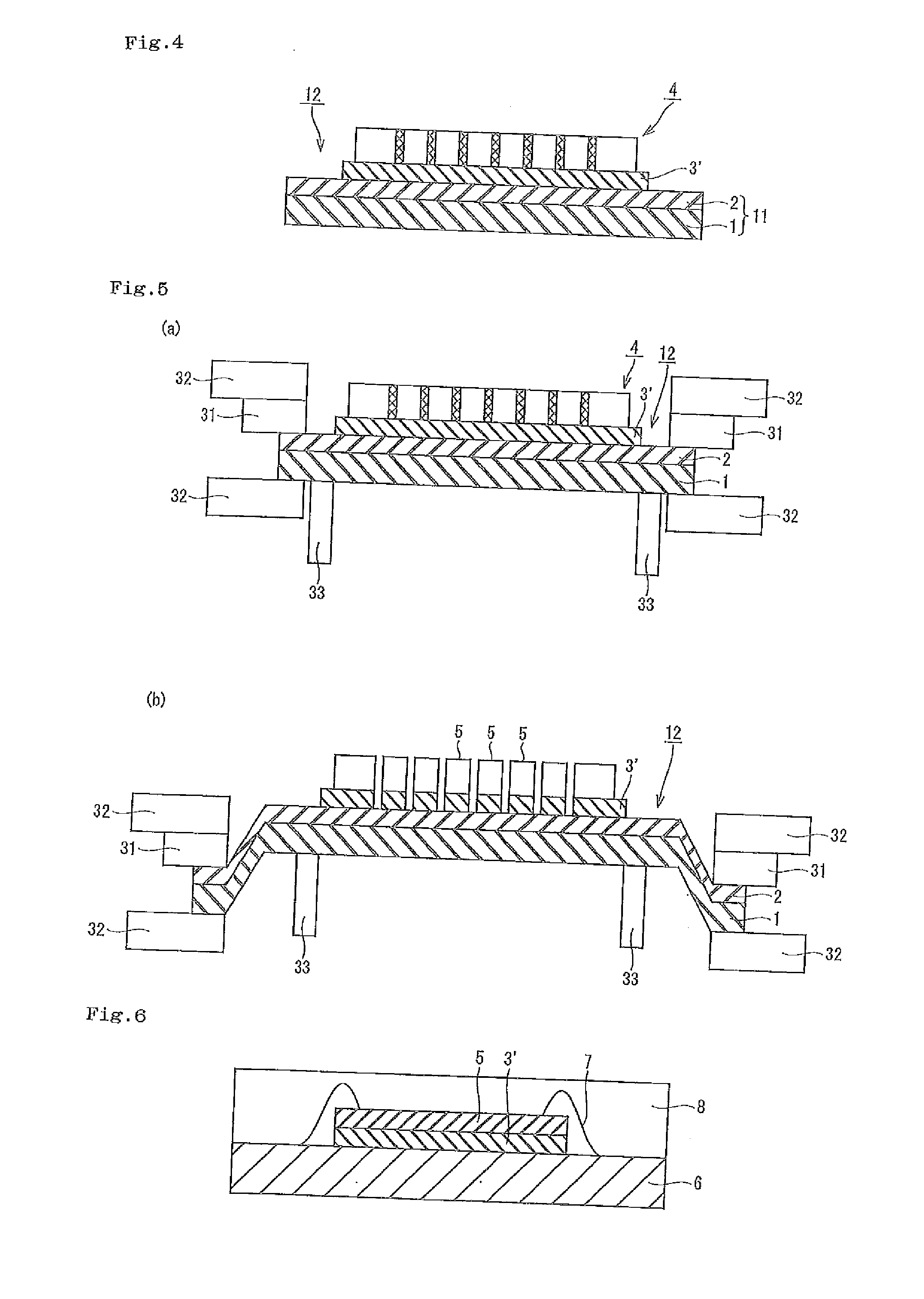
[0015]In the above-described configuration, a semiconductor chip with a die bond film is formed by forming a modified region on a semiconductor wafer by irradiating the semiconductor wafer with a laser beam, pasting the semiconductor wafer to the dicing die bond film, and breaking the semiconductor wafer at the modified region and simultaneously breaking the thermosetting type die bond film that configures the dicing die bond film at a position that corresponds to the modified region by applying a tensile force to the dicing die bond film. The obtained semiconductor chip with the die bond film is peeled from the dicing film. The peeled semiconductor chip with the die bond film is preferably used in a method of fixing the peeled semiconductor chip with the die bond film to an adherend with the die bond film interposed therebetween. The above-described method is a method by which generation of defects such as chipping that occurs especially when the semiconductor wafer is thin can be reduced. The volume resistivity of the thermosetting type die bond film is 1×10⁻³ Ω·cm or less. Therefore, a high antistatic effect can be exhibited even when the thermosetting type die bond film is used in the above-described method. Because the tensile storage modulus of the thermosetting type die bond film at −20° C. before thermal curing is 0.1 to 10 GPa, generation of chipping when the semiconductor wafer is broken at the modified region can be prevented. Further, chip fly and positional deviation of the semiconductor chip during pickup thereof can be prevented.
[0016]In the above-described configuration, a semiconductor chip with a die bond film is formed by forming grooves on a surface of a semiconductor wafer, exposing the grooves by performing backside grinding, pasting the dicing die bond film to the surface of the semiconductor wafer where the grooves are exposed, and breaking the thermosetting type die bond film that configures the dicing die bond film at a position that corresponds to the grooves by applying a tensile force to the dicing die bond film. The obtained semiconductor chip with the die bond film is peeled from the dicing film. The peeled semiconductor chip with the die bond film is preferably used in a method of fixing the peeled semiconductor chip with the die bond film to an adherend with the die bond film interposed therebetween. The above-described method is a method by which generation of defects such as chipping that occurs especially when the semiconductor wafer is thin can be reduced. The volume resistivity of the thermosetting type die bond film is 1×10⁻³ Ω·cm or less. Therefore, a high antistatic effect can be exhibited even when the thermosetting type die bond film is used in the above-described method. Because the tensile storage modulus of the thermosetting type die bond film at −20° C. before thermal curing is 0.1 to 10 GPa, chip fly and positional deviation of the semiconductor chip during pickup thereof can be prevented.

Problems solved by technology

Because of that, there has been a problem that a circuit on the semiconductor chip is broken by the generated static electricity.

Method used


Image

  • Dicing die bond film
  • Dicing die bond film
  • Dicing die bond film

Examples


example 1

[0136]An adhesive composition solution having a concentration of 23% by weight was obtained by dissolving the following (a) to (g) in methylethylketone.

[0137](a) 100 parts of an acrylic ester polymer containing ethyl acrylate-methyl methacrylate as a main component (Paracron W-197CM manufactured by Negami Chemical Industries Co., Ltd.)

[0138](b) 228 parts of an epoxy resin 1 (Epicoat 1004 manufactured by Japan Epoxy Resin Co., Ltd.)

[0139](c) 206 parts of an epoxy resin 2 (Epicoat 827 manufactured by Japan Epoxy Resin Co., Ltd.)

[0140](d) 466 parts of a phenol resin (Milex XLC-4L manufactured by Mitsui Chemicals, Inc.)

[0141](e) 400 parts of a spherical copper powder 1 (SF-Cu manufactured by Nippon Atomized Metal Powder Corporation, average particle size 10 μm)

[0142](f) 267 parts of a spherical copper powder 2 (SF-Cu manufactured by Nippon Atomized Metal Powder Corporation, average particle size 6 μm)

[0143](g) 3 parts of a curing catalyst (C11-Z manufactured by Shikoku Chemicals Corpora...

example 2

[0145]In Example 2, a die bond film B according to the present example was produced in the same manner as in Example 1 except the spherical copper powder 1 of (e) and the spherical copper powder 2 of (f) were changed to 367 parts of a spherical silver powder 1 (SFR-AG manufactured by Tokuriki Chemical Research Co., Ltd., average particle size 5 μm) and 300 parts of a spherical silver powder 2 (AgC-156I manufactured by Fukuda Metal Foil & Powder Co., Ltd., average particle size 3 μm).

example 3

[0146]In Example 3, a die bond film C according to the present example was produced in the same manner as in Example 1 except the spherical copper powder 1 of (e) and the spherical copper powder 2 of (f) were changed to 2502 parts of a spherical copper powder 1 (Cu-HWQ manufactured by Fukuda Metal Foil & Powder Co., Ltd., average particle size 5 μm) and 1500 parts of a spherical copper powder 2 (Cu-HWQ manufactured by Fukuda Metal Foil & Powder Co., Ltd., average particle size 1.5 μm).


PUM

PropertyMeasurementUnit
volume resistivityaaaaaaaaaa
tensile storage modulusaaaaaaaaaa

Abstract

The present invention provides a dicing die bond film in which peeling electrification hardly occurs and which has good tackiness and workability. The dicing die bond film of the present invention is a dicing die bond film including a dicing film and a thermosetting type die bond film provided thereon, wherein the thermosetting type die bond film contains conductive particles, the volume resistivity of the thermosetting type die bond film is 1×10⁻⁶ Ω·cm or more and 1×10⁻³ Ω·cm or less, and the tensile storage modulus of the thermosetting type die bond film at −20° C. before thermal curing is 0.1 to 10 GPa.

Description

BACKGROUND OF THE INVENTION[0001]1. Field of the Invention[0002]The present invention also relates to a dicing die bond film.[0003]2. Description of the Related Art[0004]Conventionally, a dicing die bond film including a dicing film and a thermosetting type die bond film laminated thereon is used in a process of manufacturing a semiconductor device (refer to Japanese Patent Application Laid-Open No. 2008-218571, for example). In the process of manufacturing a semiconductor device using this dicing die bond film, first, a semiconductor wafer is pasted and fixed to the dicing die bond film, and dicing is performed in this state. With this operation, the semiconductor wafer is processed into individual pieces having a prescribed size, which serves as semiconductor chips. Next, pickup of a semiconductor chip is performed to peel the semiconductor chip fixed to the dicing die bond film from the dicing film.[0005]In the pickup step, when the semiconductor chip with a die bond film is peel...

Claims


Application Information

Patent Timeline
Patent Type & Authority Applications(United States)
IPC IPC(8): H01L29/06B32B5/16B32B7/12H01L21/78C09J7/35
CPCC08K7/00C09J7/0203C09J9/02C09J2201/622C09J2203/326C09J2205/102H01L21/67132H01L23/3121H01L24/29H01L24/32H01L24/45H01L24/48H01L24/73H01L24/85H01L24/92H01L25/0657H01L2224/2929H01L2224/293H01L2224/29324H01L2224/29339H01L2224/29344H01L2224/29347H01L2224/29355H01L2224/2939H01L2224/294H01L2224/32145H01L2224/32225H01L2224/32245H01L2224/45124H01L2224/45144H01L2224/45147H01L2224/48145H01L2224/48227H01L2224/48247H01L2224/73265H01L2224/85205H01L2224/92247H01L2924/01012H01L2924/01013H01L2924/01029H01L2924/01047H01L2924/01051H01L2924/01057H01L2924/01079H01L2924/01082H01L2224/2919H01L2924/01005H01L2924/01006H01L2924/01019H01L2924/0102H01L2924/01023H01L2924/01033H01L2924/01045H01L2924/01074H01L2924/01077H01L2924/0665H01L21/6836H01L2221/68327H01L2221/68336H01L2221/6834H01L2221/68377H01L2924/01014H01L2924/01028H01L2924/10253H01L2924/15747H01L2224/48091H01L2924/3025H01L21/78H01L2924/01015Y10T428/28Y10T428/25Y10T428/2817H01L2924/00014H01L2924/00H01L2924/00012H01L2924/3512H01L2924/00011H01L2924/15788H01L2924/181H01L2924/12042C09J7/35C09J2301/312C09J2301/408
Inventor AMANO, YASUHIROMORITA, MIKIKIMURA, YUTA
Owner NITTO DENKO CORP
Learn More