Construction structures and manufacturing processes for integrated circuit wafer probe card assemblies

a technology of integrated circuit wafer and probe card, which is applied in the direction of manufacturing tools, fixed connections, instruments, etc., can solve the problems of unreliable electrical contact under use conditions, inability to reliably test the structure of the interposer and the probe card, and inability to meet the requirements of use, so as to improve the structure and process of the probe card assembly, improve the manufacturing technique, and enhance the effect of solder connection

Inactive Publication Date: 2012-02-02
CHONG FU CHIUNG +6
View PDF12 Cites 10 Cited by
  • Summary
  • Abstract
  • Description
  • Claims
  • Application Information

AI Technical Summary

Benefits of technology

[0020]Enhanced microfabricated spring contact structures and associated methods, e.g. such as for electrical contactors and interposers, comprise improvements to spring structures that extend from the substrate surface, and / or improvements to structures on or within the support substrate. Improved spring structures and processes comprise embodiments having selectively formed and etched, coated and / or plated regions, which are optionally further processed through planarization and / or annealment. Enhanced solder connections and associated processes provide a gap between substrates for componentry, and or improved manufacturing techniques using distributed spacers. Enhanced probe card assembly structures and processes provide improved planarization adjustment and thermal stability.

Problems solved by technology

With increasing numbers of I / O connections per die, the cost of testing each die becomes a greater and greater fraction of the total device cost.
Interposers, having many contacts in parallel, can be subject to contamination from particulates or other contamination layers, e.g. surface contamination layers, which may cause unreliable electrical contact under use conditions, such as including repeated mechanical and thermal cycling.
While it is desirable to increase the contact force, it is undesirable to increase contact force excessively, since the force to compress the interposer becomes too high, which may cause unacceptable mechanical deflection of the interposer and probe card structures.

Method used


Image

  • Construction structures and manufacturing processes for integrated circuit wafer probe card assemblies
  • Construction structures and manufacturing processes for integrated circuit wafer probe card assemblies
  • Construction structures and manufacturing processes for integrated circuit wafer probe card assemblies

Examples


Embodiment Construction

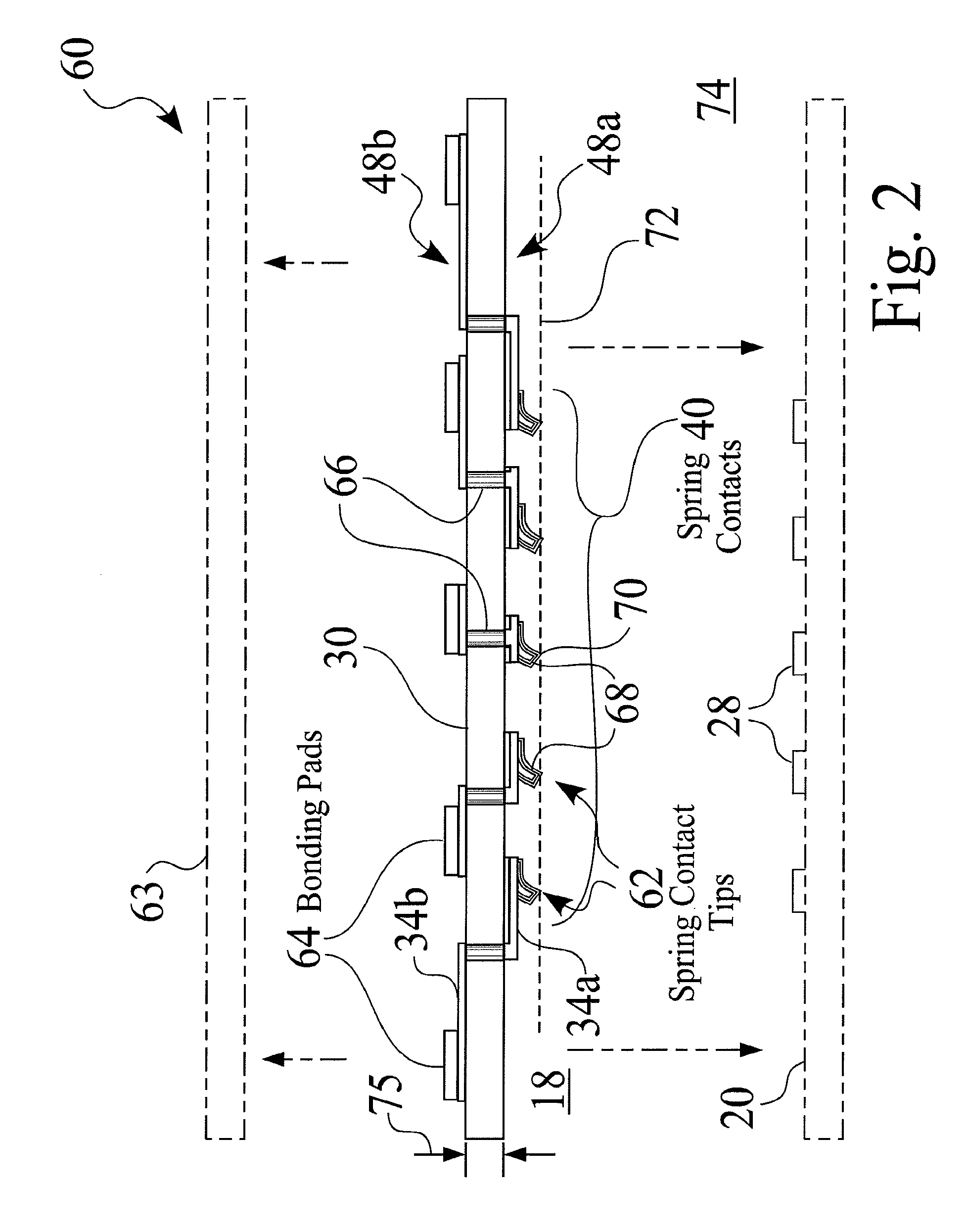
[0054]Micro-fabricated spring contacts may be fabricated with a variety of processes known to those skilled in the art. Exemplary monolithic micro-fabricated spring contacts may comprise stress metal springs that are photolithographically patterned and fabricated on a substrate using batch mode semiconductor manufacturing processes. As a result, the spring contacts are fabricated en masse, and can be fabricated with spacings equal to or less than that of semiconductor bonding pads or with spacings equal to or greater than those of printed circuit boards, i.e. functioning as an electrical signal space transformer.

[0055]Fabrication of high density arrays of spring contacts are also possible using monolithic micro-fabrication processes wherein arrays of elastic, i.e. resilient, core members, i.e. spring contact skeleton structures, are fabricated directly on a contactor substrate utilizing thick or thin film photolithographic batch mode processing techniques such as those commonly used...


PUM

PropertyMeasurementUnit
thicknessaaaaaaaaaa
thicknessaaaaaaaaaa
thicknessaaaaaaaaaa

Abstract

Enhanced microfabricated spring contact structures and associated methods, e.g. such as for electrical contactors and interposers, comprise improvements to spring structures that extend from the substrate surface, and / or improvements to structures on or within the support substrate. Improved spring structures and processes comprise embodiments having selectively formed and etched, coated and / or plated regions, which are optionally further processed through planarization and / or annealment. Enhanced solder connections and associated processes provide a gap between substrates for componentry, and or improved manufacturing techniques using distributed spacers. Enhanced probe card assembly structures and processes provide improved planarization adjustment and thermal stability.

Description

CROSS REFERENCE TO RELATED APPLICATIONS[0001]This Application is a divisional application of U.S. application Ser. No. 12 / 517,528, entitled Construction Structures and Manufacturing Processes for Integrated Circuit Wafer Probe Card Assemblies, filed 3 Jun. 2009, which is a U.S. National Phase entry of PCT / US2007 / 86394 filed 4 Dec. 2007, which claims priority to U.S. Provisional Application No. 60 / 868,535, entitled Construction Structures and Manufacturing Processes for Integrated Circuit Wafer Probe Card Assemblies, filed 4 Dec. 2006, to U.S. Provisional Application No. 60 / 898,964, entitled Structures and Processes for Fabrication of Probe Card Assemblies with Multi-Layer Interconnect, filed 31 Jan. 2007, and to U.S. Provisional Application No. 60 / 891,192, entitled Fine Pitch Probe Card Having Rapid Fabrication Cycle, filed 22 Feb. 2007[0002]Each of the aforementioned documents is incorporated herein in its entirety by this reference thereto.FIELD OF THE INVENTION[0003]The present i...

Claims


Application Information

Patent Timeline
Patent Type & Authority Applications(United States)
IPC IPC(8): B23P11/00
CPCG01R1/07342G01R3/00G01R31/2889Y10T29/49826H05K7/1061H01R12/718H01R12/57
Inventor CHONG, FU CHIUNGBOTTOMS, W.R.CHIEH, ERH-KONGLITZA, ANNAMCKAY, DOUGLAS L.MILTER, ROMAN L.LI, SHA
Owner CHONG FU CHIUNG
Why Eureka
Try Eureka