Chalcogenide-based materials and methods of making such materials under vacuum using post-chalcogenization techniques
a technology of chalcogenide-based materials and vacuum evaporation, which is applied in the direction of vacuum evaporation coating, solid-state diffusion coating, coating, etc., can solve the problems of difficult industrial application of conventional evaporation methods, inflexible, and rigidity of chalcogenide-based absorbers, etc., and achieves high quality.
- Summary
- Abstract
- Description
- Claims
- Application Information
AI Technical Summary
Benefits of technology
Problems solved by technology
Method used
Image
Examples
example 1
Fabrication of CIGS Solar Cell in a Roll-to-Roll Tool
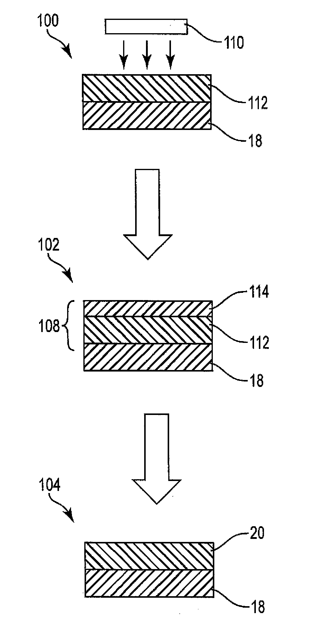
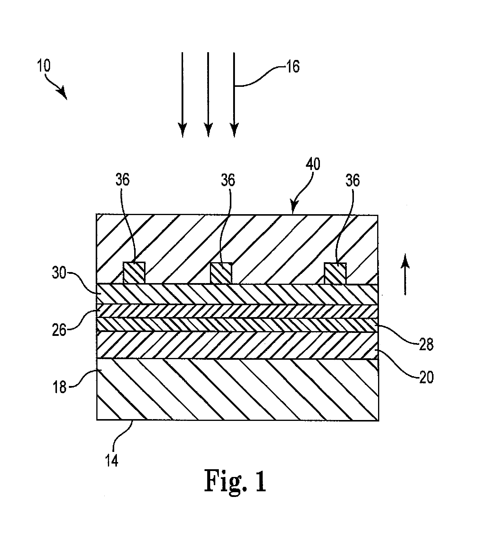
[0069]Substrate preparation:[0070]A roll of 430 series stainless steel is loaded into a continuous roll-to-roll vacuum sputtering system. This active side of the web is first cleaned with ion etching and then is coated by magnetron sputtering with a Nb barrier layer, a dual layer of Mo for a back contact and a NaF layer to act as a sodium source. The back side of the web is coated with Cr as an adhesion layer and Mo to act as a sacrificial layer during the selenization process.[0071]Target arrangement[0072]The web is then translated into a Cu:In:Ga precursor sputtering chamber. Seven pulsed DC magnetrons are arranged in four zones. Each zone has individual gas control. The web is transported sequentially through the four zones. Each of the first, third, and fourth zones has 2 magnetrons. The second zone has a single magnetron. In this example, all magnetrons are adjusted to sputter parallel to the web. The web moves from magnetron...
example 2
Fabrication of Tetragonal CIGS in the Presence of H2S Gas (H2S) on a Cluster Tool at 6.6e-3 mBar and 350 C
[0081]Substrate preparation:[0082]A stainless steel coupon is first cleaned by sonication in solvent baths and dried with dry N2 gas and loaded into a multi-chamber vacuum deposition system. The face of the substrate is further cleaned using 300W RF plasma etching in Argon. The substrate is then transferred under vacuum to a second chamber where a niobium adhesion layer and molybdenum back contact layer are deposited by sputtering. The sample is removed from vacuum.[0083]Targets[0084]The substrate is later introduced into a precursor sputtering chamber comprising a single, commercially available Cu:In:Ga alloy target tilted off-axis with respect to the substrate to give a more uniform coating thickness. The target is 45:42:13 Cu:In:Ga. The sample is rotated during deposition.[0085]Deposition conditions The CIG precursor film is sputtered at 75 Watts, in ˜4e-3 mBar in Argon at am...
example 3
Formation of CIGS in H2Se at 10 mT, 25× cap, 350 C
[0092]Substrate preparation[0093]The substrate is prepared as in Example 2.[0094]Target arrangement.[0095]Targets are used according to Example 2.[0096]Deposition conditions[0097]Deposition of a CIG precursor on the substrate is carried out as in Example 2.[0098]Description of cap formation on precursor[0099]A Se cap is formed on the CIG precursor as in Example 2.[0100]Anneal conditions.[0101]After application of the selenium cap, the substrate bearing the CIG-Se stack is removed from vacuum and transferred to a selenization chamber. In this chamber, the substrate is suspended face down and heated from the back-side with a radiative graphite element. The system has water-cooled walls (2Se gas prior to heating. The substrate ramped up to >350° C. at 20° C. / min by setting the power supply for the graphite heater at a previously determined power duty cycle value. The temperature of the substrate is maintained at >300° C. for 20 minutes ...
PUM
| Property | Measurement | Unit |
|---|---|---|
| pressure | aaaaa | aaaaa |
| temperature | aaaaa | aaaaa |
| pressure | aaaaa | aaaaa |
Abstract
Description
Claims
Application Information
 - Generate Ideas
- Intellectual Property
- Life Sciences
- Materials
- Tech Scout
- Unparalleled Data Quality
- Higher Quality Content
- 60% Fewer Hallucinations
Browse by: Latest US Patents, China's latest patents, Technical Efficacy Thesaurus, Application Domain, Technology Topic, Popular Technical Reports.
© 2025 PatSnap. All rights reserved.Legal|Privacy policy|Modern Slavery Act Transparency Statement|Sitemap|About US| Contact US: help@patsnap.com


