EUV Lithography Device and Method For Processing An Optical Element

Active Publication Date: 2011-11-17
CARL ZEISS SMT GMBH
View PDF10 Cites 30 Cited by
  • Summary
  • Abstract
  • Description
  • Claims
  • Application Information

AI Technical Summary

Benefits of technology

[0011]An object of the invention is to provide an EUV lithography device and a method for processing an optical element, in particular a mask, which allow rapid and effective removal of particularly local contamination and, where applicable, correction of defects.SUMMARY
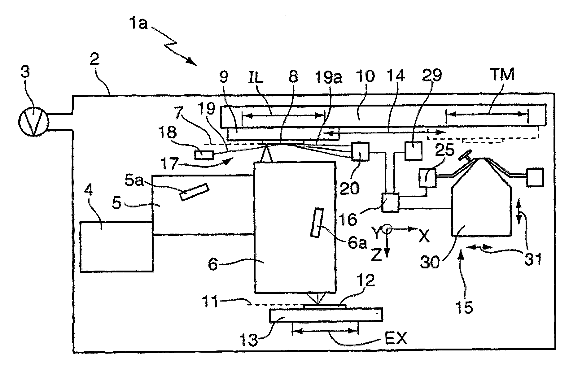
[0015]Owing to the gas nozzle(s), a localised application of the gas stream to the surface of the optical element to be processed can be brought about, it being possible to activate at least one gas component of the gas stream by radiation, in particular in the UV, DUV or visible range, by a particle beam, preferably an electron beam, and / or by high-frequency excitation. In this instance, the gas stream can be activated in the region of the optical elements to be cleaned and the gas stream can be discharged from the gas nozzle, in particular with little spacing from the surface to be cleaned. A highly locally selective processing operation is thereby possible.
[0020]In another embodiment, the processing device comprises an optical unit for expanding, focusing and / or redirecting the radiation or the particle beam. The electromagnetic radiation which is produced, for example, by a laser, can be redirected, expanded or focused by way of conventional lenses or mirrors. If the particle beam is a beam of charged particles, for example, an electron beam, it can also be redirected by conventional (electron or ion) optical units for producing electrical and / or magnetic fields. The expansion / focusing is advantageous in order to adjust the size of the point of impact of the radiation or the particle beam because the processing action and in particular the cleaning action of the gas stream is concentrated around the point of impact.
[0027]In one embodiment, the EUV lithography device comprises a movement device for moving the processing device relative to the optical element arranged at the processing position. In this instance, it is possible to configure the processing device for scanning the surface of the optical element and to provide it with a suitable displacement device. Alternatively or additionally, in particular when a mask is processed as the optical element, the element itself can be displaced at the processing position in order to allow scanning processing of the surface. However, the processing position can also correspond to the location at which the optical element is arranged during exposure operation in order to allow processing in situ. Alternatively, the optical element can also be moved from the position, at which it is arranged during exposure operation, into a processing position by a transport device, which has been found to be advantageous particularly when the mask is processed.
[0028]In another embodiment, the EUV lithography device comprises a transport device for moving the mask from the illumination position into the processing position. The inventors have recognised that correction complexity and processing operations of the mask are to be expected more often in EUV lithography than in conventional lithography, for example, at 193 nm, so that the integration of the correction function for defects in a mask in an EUV processing station is connected with a very large advantage in terms of time. In this case, the sensitive mask does not have to be transported between different spatially separate systems by using transport boxes, unloaded and loaded, for which the vacuum has to be interrupted which may result in additional contamination in the mask. Since the mask does not have to be taken out of the projection exposure system having an integrated correction function and processing station during processing according to the invention, the risk of contamination owing to particles or damage owing to the mask being handled is also consequently reduced.
[0029]When the mask is transported from the illumination position to the processing position, the vacuum in the EUV lithography device is not interrupted so that the risk of additional contamination may be avoided. It is further possible to configure the transport device so that, when the mask is transported from the processing position to the illumination position (and back), it is not necessary to carry out reconfiguration, that is to say, no new orientation of the coordinate system of the mask in relation to the coordinate system of the EUV lithography device, so that the exposure or processing operation can be carried out directly.

Problems solved by technology

The inventors have recognised that extensive introduction of cleaning gas, for example, atomic hydrogen, is not favourable for cleaning optical elements in EUV lithography devices because in this instance larger regions of the vacuum environment of the EUV lithography device typically come into contact with the cleaning gas than is absolutely necessary, which may result in degradation of material on optical surfaces in the vacuum environment which are not intended to be cleaned.
This is the case, for example, in the so-called “hydrogen induced outgassing” (HIO) effect, in which volatile hydrides, in particular of metals such as tin or zinc, but also of sulphur, are produced by the cleaning with atomic hydrogen and become dispersed in the EUV lithography device and deposited in an undesirable manner as (metal) deposits on the surfaces of optical elements, which may result in a substantial loss in transmission in the lithography device.

Method used


Image

  • EUV Lithography Device and Method For Processing An Optical Element
  • EUV Lithography Device and Method For Processing An Optical Element
  • EUV Lithography Device and Method For Processing An Optical Element

Examples


Embodiment Construction

[0045]FIGS. 1a-c schematically illustrate three embodiments of EUV lithography devices 1a-c which have a housing 2, with which a vacuum generating unit 3 (vacuum pump) for generating a vacuum environment is associated and which produces in the housing 2 a residual gas atmosphere having a total pressure in a range from approximately 10−3 mbar to 0.1 mbar. The housing 2 is subdivided into three housing portions 4, 5, 6 which are figuratively illustrated in FIGS. 1a-c in accordance with the optical function of the optical elements arranged therein, that is, a first housing portion 4 which is also referred to as the light generating unit and which comprises a plasma light source and an EUV collector mirror for focusing the illumination radiation. There is arranged in the adjacent second housing portion 5 the illumination system which serves to generate an image field which is as homogeneous as possible in an object plane 7, in which a mask 8 having a structure (not illustrated) which is...


PUM


Abstract

An EUV lithography device including an illumination device for illuminating a mask at an illumination position in the EUV lithography device and a projection device for imaging a structure provided on the mask onto a light-sensitive substrate. The EUV lithography device has a processing device (15) for processing an optical element (6a), in particular the mask, preferably in a locally resolved manner, at a processing position in the EUV lithography device. For activating at least one gas component of the gas stream (27), the processing device (15) comprises a particle generator (30) for generating a particle beam, in particular an electron beam (30a), and / or a high-frequency generator.

Description

CROSS-REFERENCE TO RELATED PATENT APPLICATIONS[0001]This is a Continuation of International Application PCT / EP2009 / 007411, with an international filing date of Oct. 15, 2009, which was published under PCT Article 21(2) in German, which claims priority under 35 U.S.C. § 119(a) to German Patent Application No. 10 2008 042 857.4, filed on Oct. 15, 2008; this application also claims the benefit under 35 U.S.C. § 119(e)(1) of U.S. Provisional Application No. 61 / 105,568, filed Oct. 15, 2008. The entire contents of the International Application and the two priority applications are hereby incorporated into the present application by reference.BACKGROUND OF THE INVENTION[0002]The invention relates to an EUV lithography device comprising: an illumination device for illuminating a mask at an illumination position in the EUV lithography device and a projection device for imaging a structure provided on the mask onto a light-sensitive substrate. The invention also relates to a method for proces...

Claims


Application Information

Patent Timeline
IPC IPC(8): G03B27/42G03F1/82G03F1/86
CPCG03F1/82G03F1/86G03F7/70925G03F7/7085G03F7/70866G03F7/70733G03F1/68G03F7/2026G03F7/70058H01L21/0273H01L21/0274
Inventor SINGER, WOLFGANGKWAN, YIM-BUN-PATRICKSCHMIDT, STEFAN-WOLFGANGEHM, DIRK HEINRICHKRAUS, DIETERWIESNER, STEFANKOEHLER, STEFANCZAP, ALMUTCHUNG, HIN YIU ANTHONY
Owner CARL ZEISS SMT GMBH
Why Eureka
Try Eureka