Charge-transporting varnishes
a charge-transporting varnish and varnish technology, applied in the field of charge-transporting varnishes, can solve the problems of no case of adding a silane compound to charge-transporting varnishes including low-molecular weight oligomers, and the difficulty of homogeneous film formation, etc., to achieve excellent emission efficiency and luminance characteristics, good thin film forming abolity, and high flatness
- Summary
- Abstract
- Description
- Claims
- Application Information
AI Technical Summary
Benefits of technology
Problems solved by technology
Method used
Image
Examples
example 1
[0334]0.150 g (0.340 mmol) of PTA synthesized in Reference 1 0.307 g and (0.340 mmol) of NSO-2 synthesized in Reference 2 were completely dissolved in 17.5 g of DMI in a nitrogen atmosphere. The resulting solution was mixed with 15.0 g of 2,3-BD and then with 7.5 g of nHAc and agitated. Finally, 0.046 g of a mixed solvent of trimethoxy(3,3,3-trifluoropropyl)silane and tri(methoxyphenyl)silane at 1:2 (ratio by weight) was added, thereby preparing a charge-transporting varnish (solid content: 1.5 wt %).
[0335]Using the prepared varnish, a charge-transporting thin film was formed in the same manner and under the same conditions as in Comparative Example 1.
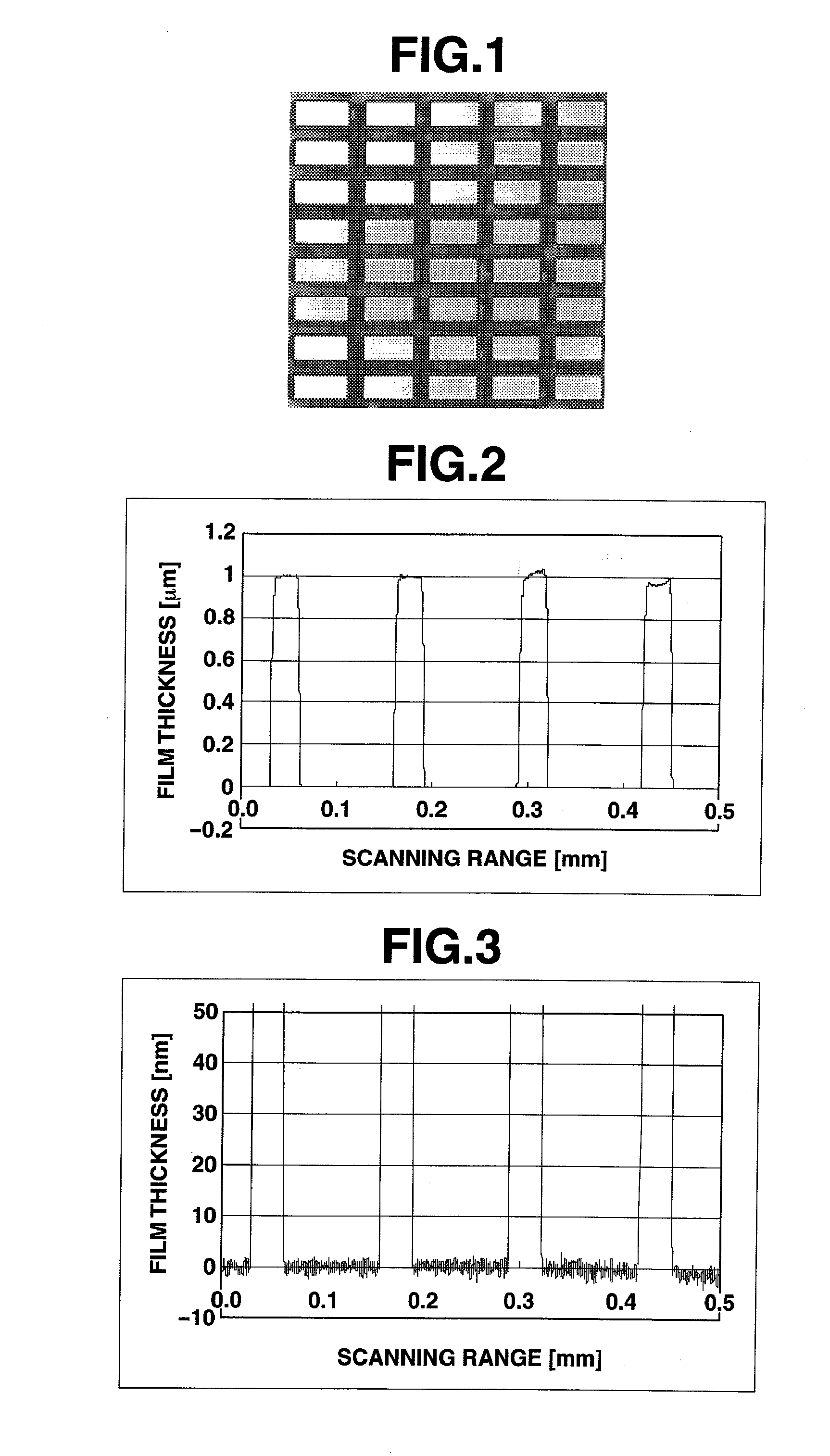
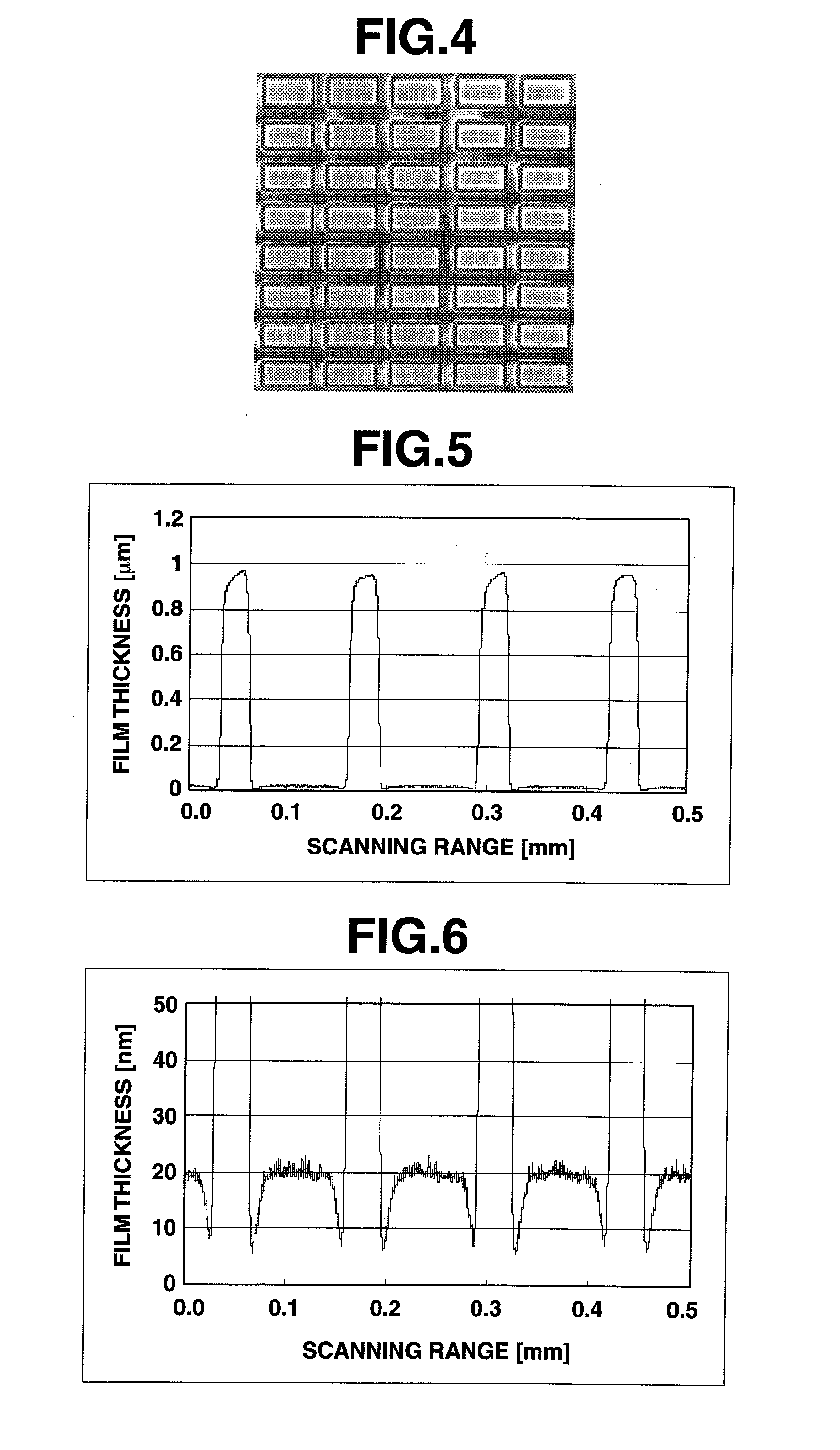
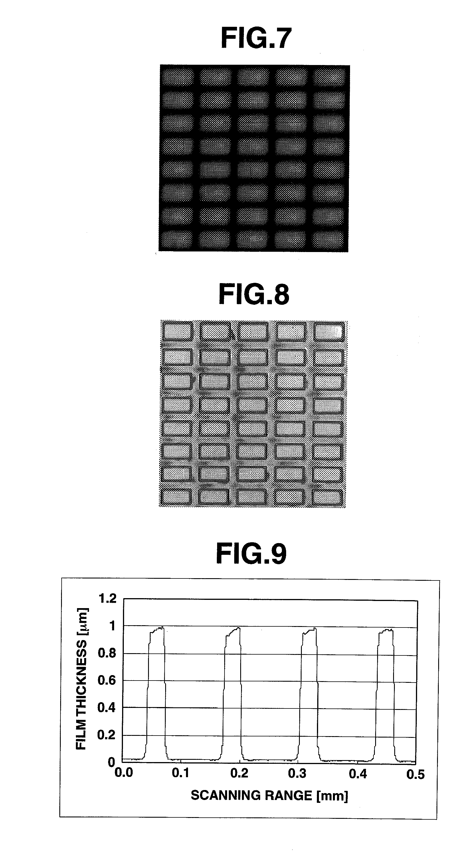
[0336]FIG. 8 shows a confocal laser microphotograph of the charge-transporting thin film coated onto a structure-bearing substrate. FIGS. 9 and 10 show the results of measurement of a thickness distribution of the charge-transporting thin film of Example 1.
[0337]Next, the substrate was introduced into a vacuum deposition apparatus, fol...
example 2
[0342]0.0601 g (0.136 mmol) of PTA synthesized in Reference 1 and 0.1226 g (0.136 mmol) of NSO-2 synthesized in Reference 2 were completely dissolved in 14.0 g of DMI in an atmosphere of nitrogen. The resulting solution was admixed with 6.0 g of CHA and subsequently with 2.0 g of 2,3-BD and agitated. Finally, 0.018 g of a mixed solvent of trimethoxy(3,3,3-trifluoropropyl)silane and tri(methoxyphenyl)silane at 1:2 (ratio by weight) was added, thereby preparing a charge-transporting varnish (solid content: 1.5 wt %).
[0343]Using this varnish, a uniform thin film having a thickness of about 30 nm was formed on an ITO glass substrate by a spin coating method, followed by introduction into a vacuum deposition apparatus and successive deposition of α-NPD, Alq3, LiF and Al in the same manner as in Comparative Example 1, thereby obtaining an OLED element.
[0344]The characteristics of the OLED elements obtained in Example 2 and Comparative Example 2 were evaluated. The results are shown in FIG...
PUM
| Property | Measurement | Unit |
|---|---|---|
| Mass | aaaaa | aaaaa |
| Weight | aaaaa | aaaaa |
| Electric charge | aaaaa | aaaaa |
Abstract
Description
Claims
Application Information
 - R&D
- Intellectual Property
- Life Sciences
- Materials
- Tech Scout
- Unparalleled Data Quality
- Higher Quality Content
- 60% Fewer Hallucinations
Browse by: Latest US Patents, China's latest patents, Technical Efficacy Thesaurus, Application Domain, Technology Topic, Popular Technical Reports.
© 2025 PatSnap. All rights reserved.Legal|Privacy policy|Modern Slavery Act Transparency Statement|Sitemap|About US| Contact US: help@patsnap.com


