
Semiconductor package having electrical connecting structures and fabrication method thereof

a technology of semiconductors and electrical connections, applied in the field of packaging structures and fabrication methods, can solve the problems of poor electrical connection between the package and the printed circuit board, adversely affecting the electrical performance of the package, electrical leakage and even short circuit at the interface, etc., to prolong the permeation path of solder material or moisture into the package, reduce the length of the bonding wire, and enhance the adhesion strength of the solder mask layer

Active Publication Date: 2011-06-30
SILICONWARE PRECISION IND CO LTD
View PDF7 Cites 14 Cited by
  • Summary
  • Abstract
  • Description
  • Claims
  • Application Information

AI Technical Summary

Benefits of technology

The present invention provides a semiconductor package with electrical connecting structures that have improved reliability and reduced packaging costs. The package includes a conductive layer with a plurality of traces, a chip mounted on the conductive layer, and a plurality of bonding wires and encapsulant. The encapsulant has a plurality of cavities that expose at least a portion of the conductive layer. A solder mask layer is formed on the exposed surface of the conductive layer and a bottom surface of the encapsulant, with openings for exposing the trace ends. The semiconductor package also includes a fabrication method for the same. The technical effects of the invention include improved reliability, reduced packaging costs, and more efficient use of space.

Problems solved by technology

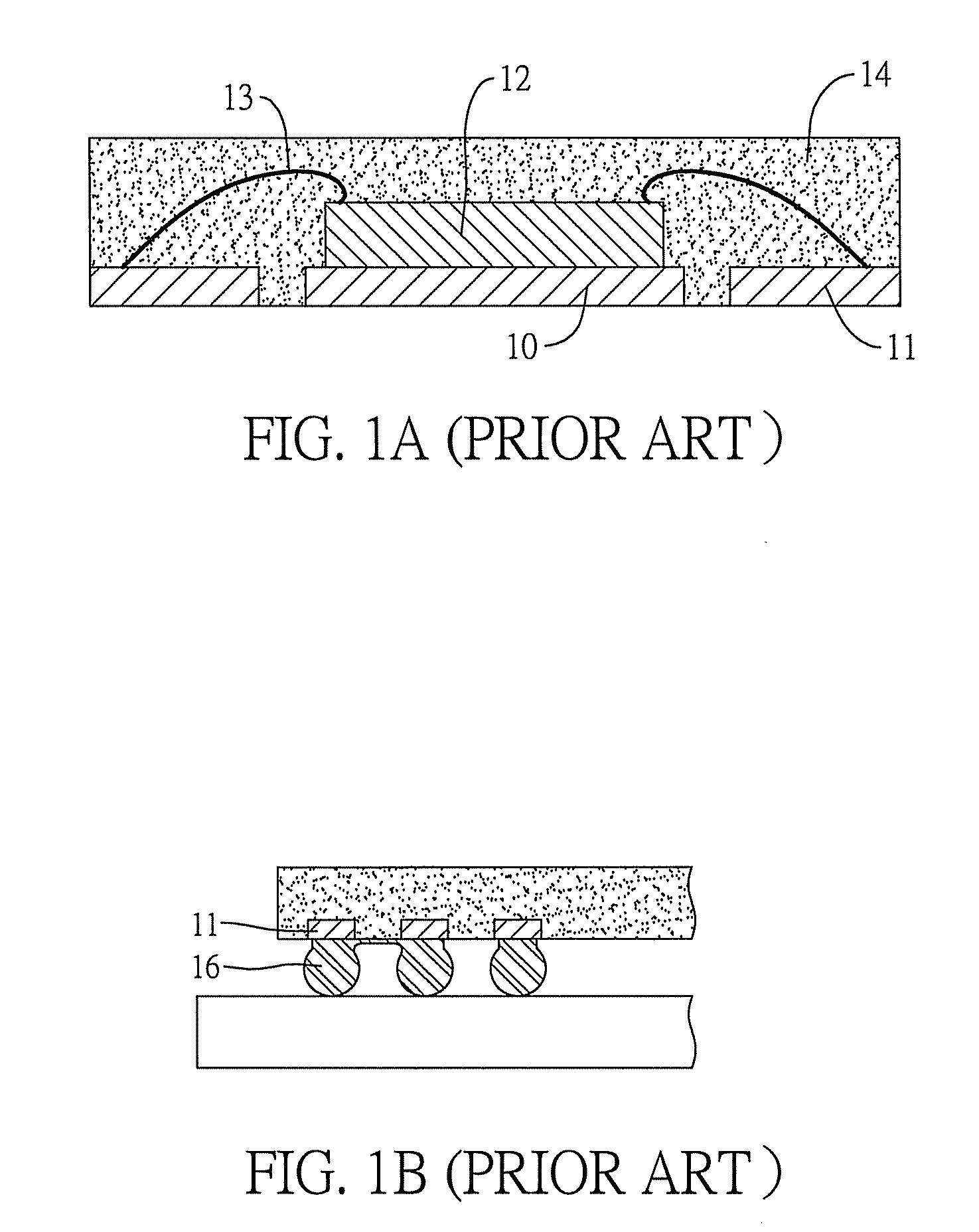
However, as shown in FIG. 1B, since the exposed surfaces of the leads 11 are flush with the encapsulant 14, when solder balls are mounted on the leads 11 for electrically connecting an external printed circuit board, solder bridge is likely to be formed between adjacent solder balls, thereby resulting in poor electrical connection between the package and the printed circuit board.
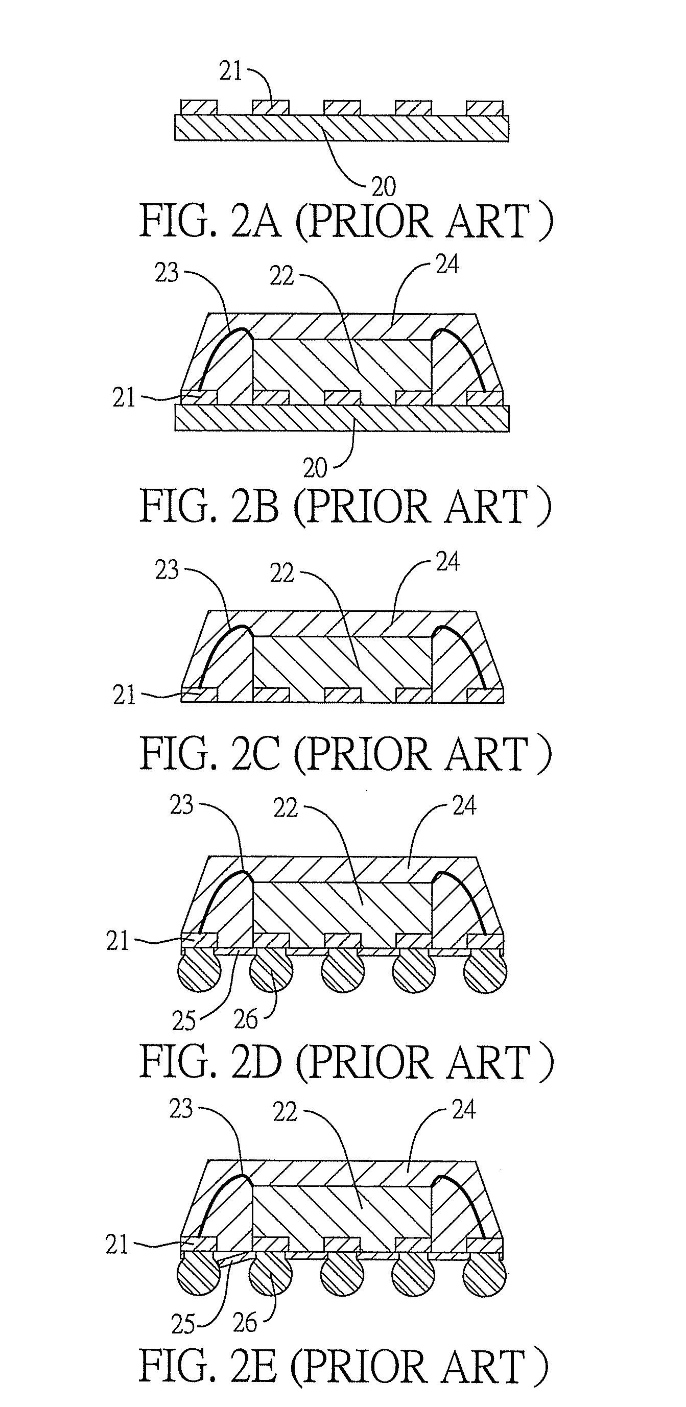
As such, moisture can easily permeate therebetween and thus causes electrical leakage of the electroplated projections 21, thereby adversely affecting the electrical performance of the package.
Furthermore, a soldering process or thermal cycling in practical applications may cause permeation of solder material into the interface between the antioxidation coating 25 and the encapsulant 24, thus resulting in electrical leakage and even short circuit at the interface.

Method used


Image

  • Semiconductor package having electrical connecting structures and fabrication method thereof
  • Semiconductor package having electrical connecting structures and fabrication method thereof
  • Semiconductor package having electrical connecting structures and fabrication method thereof

Examples


Embodiment Construction

[0035]The following illustrative embodiments are provided to illustrate the disclosure of the present invention, these and other advantages and effects can be apparent to those in the art after reading this specification.

[0036]It should be noted that terms referring to relativity, such as “top” and “bottom”, used in the disclosure are intended to describe relative connecting relationship of components in a semiconductor package but are not intended to limit the scope of the present invention.

[0037]FIGS. 3A to 3H show a fabrication method of a semiconductor package having electrical connecting structures according to an embodiment of the present invention.

[0038]As shown in FIG. 3A, a metal board 30 with a plurality of substrate units 31 is provided. A resist layer 32 is formed on the metal board 30. A plurality of openings 320 are formed in the resist layer 32 to expose a portion of the metal board 30. In the present embodiment, the metal board 30 is made of copper.

[0039]As shown in ...


PUM


Abstract

A semiconductor package having electrical connecting structures includes: a conductive layer having a die pad and traces surrounding the die pad; a chip; bonding wires; an encapsulant with a plurality of cavities having a depth greater than the thickness of the die pad and traces for embedding the die pad and the traces therein, and the cavities exposing the die pad and the traces; a solder mask layer formed in the cavities and having a plurality of openings for exposing the trace ends and a portion of the die pad; and solder balls formed in the openings and electrically connected to the trace ends. Engaging the solder mask layer with the encapsulant enhances adhesion strength of the solder mask layer so as to prolong the moisture permeation path and enhance package reliability.

Description

BACKGROUND OF THE INVENTION[0001]1. Field of the Invention[0002]The present invention relates generally to package structures and fabrication methods thereof, and more particularly, to a QFN (Quad Flat Non-leaded) semiconductor package having electrical connecting structures and a fabrication method thereof.[0003]2. Description of Related Art[0004]Conventionally, a lead frame is used as a chip carrier for carrying a chip so as to form a semiconductor package. The lead frame essentially comprises a die pad and a plurality of leads formed at the periphery of the die pad. A chip is adhered to the die pad and electrically connected to the leads through a plurality of bonding wires. The chip, the die pad, the bonding wires and inner sections of the leads are then encapsulated by a packaging resin so as to form a semiconductor package having a lead frame.[0005]Developing high integration and high density package structures has become a goal of semiconductor industries. Carriers for chip s...

Claims


Application Information

Patent Timeline
Patent Type & Authority Applications(United States)
IPC IPC(8): H01L23/49H01L21/00
CPCH01L21/568H01L2924/15151H01L24/48H01L24/85H01L2224/16H01L2224/45144H01L2224/48091H01L2224/48227H01L2224/48247H01L2224/484H01L2224/48599H01L2224/85001H01L2224/85444H01L2224/85455H01L2224/85464H01L2924/01028H01L2924/01029H01L2924/01046H01L2924/0105H01L2924/01079H01L2924/01082H01L2924/014H01L2924/15311H01L23/3128H01L2924/01033H01L2924/00014H01L21/78H01L23/4952H01L2224/78H01L2224/48644H01L2224/48655H01L2224/48664H01L24/45H01L2924/181H01L2924/00H01L2224/05599H01L2924/00012
Inventor LIN, PANG-CHUNLI, CHUN-YUANTANG, FU-DIHUANG, CHIEN-PINGKE, CHUN-CHI
Owner SILICONWARE PRECISION IND CO LTD
Learn More