Apparatus and method for predetermined component placement to a target platform

a technology of predetermined components and target platforms, applied in the field of assembly techniques, can solve the problems of increasing the operation speed of integrated circuits (ic), increasing the number of power and ground and increasing the number of pins in packaged devices or components. , to achieve the effect of accurate control, higher component yield and larger toleran

Inactive Publication Date: 2011-05-26
WINTEC IND INC
View PDF50 Cites 19 Cited by
  • Summary
  • Abstract
  • Description
  • Claims
  • Application Information

AI Technical Summary

Benefits of technology

[0009]The present invention relates in general to assembly techniques. According to the present invention, the alignment and probing techniques to improve the accuracy of component placement in assembly are described. More particularly, the invention includes methods and structures to detect and improve the component placement accuracy on a target platform by incorporating alignment marks on components and reference marks on target platforms. Proper alignment is assessed with various probing techniques. A set of sensors grouped in an array to form a multiple-sensor probe is used to detect the deviation of displaced components on a target platform. Merely by way of example, the invention may be applied to place components onto electronic substrates for the manufacture of electronic systems. However, it should be recognized that the invention has a much broader range of applicability, such the precision alignment of a set of different objects.
[0011]In a specific embodiment, an alignment mark is a reference area on a component that an external probe can use to monitor the accuracy of a component placement on a target platform. The alignment mark incorporated on the component can be a conduction path connecting a top surface area to a bottom surface area of the component as a direct alignment mark, or it can be a different conduction path connecting two surface areas on the bottom of the component as an indirect alignment mark. Besides being a conduction path within the component, the alignment mark can also be a simple surface marking on the component, depending upon the probing method used. The structure of an alignment mark can be a simple geometric structure or a set of geometric structures.
[0013]In preferred embodiments, the present invention provides probe solutions for improving the accuracy in component placement. The probe can be a single-sensor probe or it can be an array of sensors. A single-sensor probe can detect the accuracy of a component placement and the status of a component's contact condition on a target platform. A probe composing of an array of sensors to become a multiple-sensor probe can adjust the deviation of a displaced component by aligning the one or more alignment marks on the component to the probe position that has been aligned to a reference mark. A multiple sensor probe can detect the deviation of a component and feed back the information to the placement equipment to fix the position deviation. While a single alignment mark can fix the component displacement error, two alignment marks can fix the placement orientation error. The probe can be a resistance probe, a capacitance probe, an optical probe, or any combination thereof. The resistance probe is for on / off measurements, the capacitance probe is for measuring the relative overlapping area between a sensor surface and a target reference, and the optical probe is for measuring the reflection from a target reference. The resistance probe is a contact probe. The capacitance probe and optical probe are non-contact probes. The range of active sensors on the multiple-sensor probe can be determined automatically by sensing the size of a target reference mark.
[0016]Since the spatial relationship of alignment marks to the associated contact array can be accurately controlled in the device fabrication or component packaging process, a fixed spatial relationship between an alignment mark and a contact array on a device or package can be ensured. This allows a package with a minor obliquity in its physical outline (an oblique package) or a bare die not perfectly centered-cut along the scribing line between adjacent dies (off-center-cut die) to still be used for assembly. This is because in assembly the component placement can rely on the position of the alignment marks, rather than counting on the geometrical tolerance of the package outline. In a specific embodiment, the present invention provides a method for mounting a physically out-of-specification device or package on a prospective contact region on a PCB or target platform. Many physically out-of-specification devices which previously would have caused a misalignment problem in assembly no longer need to be rejected. A larger tolerance in the die cutting of device or in the molding of component package means a higher component yield.
[0017]Many benefits can be achieved by way of the present invention over conventional techniques. The present technique provides an easy to use process that relies upon conventional technology. In some embodiments, the method provides a mean to improve yields, reduce rework, and enhance placement accuracy. Additionally, the method provides a process that is compatible with conventional process technology without substantial modifications to the conventional equipment and processes. The present invention is especially useful for the devices with ultra-fine contact pitch and contact count exceeding hundreds or even a thousand.
[0018]Moreover, the invention provides a method for monitoring the placement of devices packaged with anisotropic conductive elastomer (ACE) as an interconnect interface. It enables the assembly of non-solder-ball based packaged devices onto a target platform or PCB effectively and precisely for a variety of applications. The anisotropic conductive elastomer contains a sea of tiny conducting metal tubes embedded in an elastic insulating silicone membrane that conducts current only in a certain direction. It has been used as an interconnect in high density and high pin count test sockets to offer excellent contact, repeatability, and high frequency characteristics in IC device tests. It is feasible to be used as the interface interconnect for devices and packages. A device or component laminated with ACE can be directly mounted onto a target substrate. A clamp shell can be used to hold the devices together without the need of soldering the devices onto a target substrate if an accurate placement can be achieved. The alignment technique can make the assembly of ACE laminated devices on electronics system feasible.

Problems solved by technology

As the complexity and the operation speed of integrated circuits (IC) increase, it is not unusual to see an increasing number of devices with pin-counts exceeding hundreds or even a thousand.
For example, high-speed designs requires many power and ground pins.
Many if not all of these tend to increase the number of pins in a packaged device or component.
The reduced pin-pitch poses a challenge for the placement equipment to place components accurately on a target platform, such as a printed circuit board (PCB), especially if the pin pitch is smaller than 0.5 mm.
Without proper feedback, the accuracy of the component placement is uncertain.
As the accumulative error is getting closer to the pitch size of the contact array, placing a component accurately on a PCB is becoming a greater challenge.
It is not uncommon to encounter component placement problems in a surface mount assembly line, especially for the placement of fine-pitch components.
For example, if a BGA component is inaccurately placed on a PCB, it could cause the BGA's contact array to deviate from the ideal land pattern location, resulting in either inadequate soldering or solder bridging to adjacent pads on the PCB.
A rework to fix these problems is tedious and expensive.
It is even worse for the rework of a pricey, high pin-count component on a high density PCB.
However, there is no handy method for users or manufacturers to monitor if a chip has been properly inserted in the socket or if the chip is in good contact with the receptacle inside the socket.

Method used


Image

  • Apparatus and method for predetermined component placement to a target platform
  • Apparatus and method for predetermined component placement to a target platform
  • Apparatus and method for predetermined component placement to a target platform

Examples


Embodiment Construction

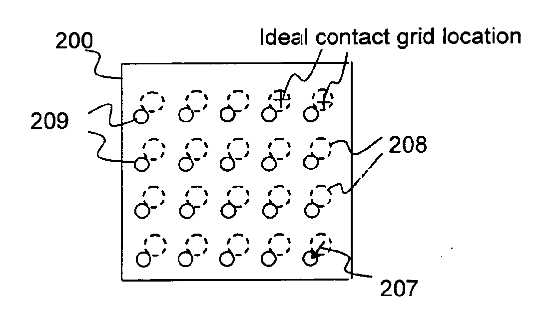
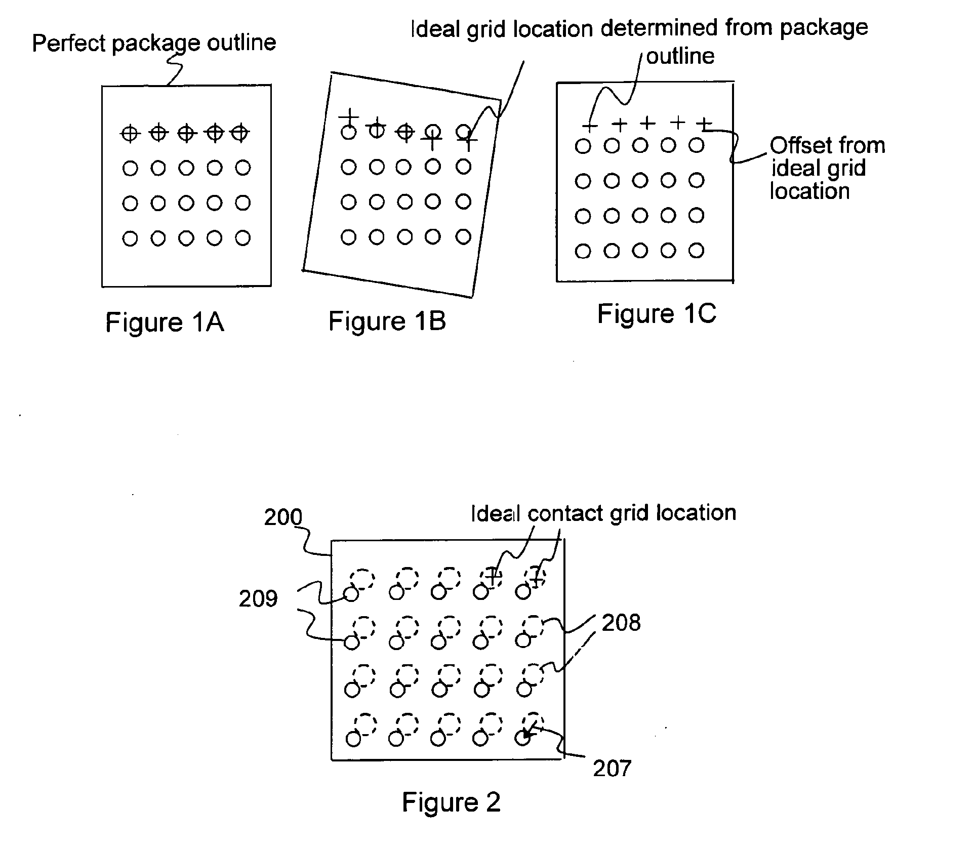
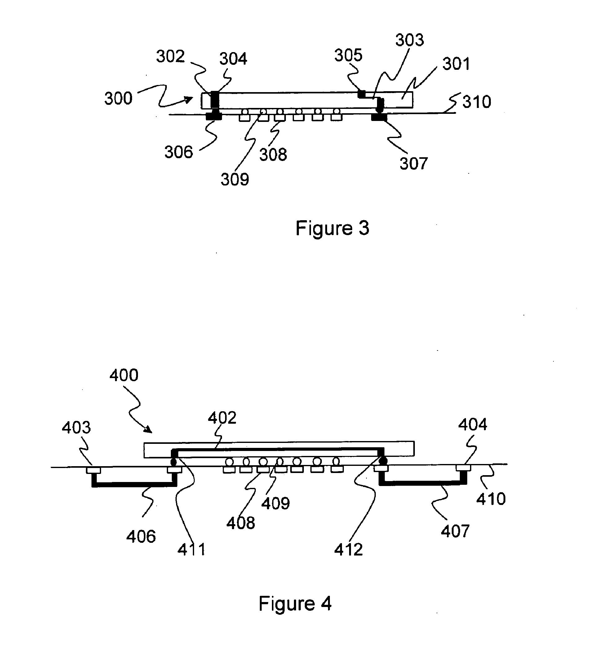
[0043]According to the present invention, alignment and probing techniques to improve the component placement accuracy during assembly are described. More particularly, the invention includes methods and structures to detect and improve the component placement accuracy on a target platform by incorporating alignment marks on a component and reference marks on a target platform with various probing techniques. A set of sensors grouped in an array to form a multiple-sensor probe can detect the deviation of displaced components in assembly. Merely by way of example, the invention can be applied to placing packaged semiconductor devices onto electronic substrates for the manufacture of electronic systems. But it would be recognized that the invention has a much broader range of applicability. Further details of the present invention can be found throughout the present specification and more particularly below.

Alignment Mark

[0044]According to preferred embodiments, an alignment mark is a...


PUM

PropertyMeasurementUnit
pitch sizeaaaaaaaaaa
densityaaaaaaaaaa
surface areaaaaaaaaaaa

Abstract

The present invention relates generally to assembly techniques. According to the present invention, the alignment and probing techniques to improve the accuracy of component placement in assembly are described. More particularly, the invention includes methods and structures to detect and improve the component placement accuracy on a target platform by incorporating alignment marks on component and reference marks on target platform under various probing techniques. A set of sensors grouped in any array to form a multiple-sensor probe can detect the deviation of displaced components in assembly.

Description

CROSS-REFERENCES TO RELATED APPLICATION[0001]This application is a continuation of U.S. application Ser. No. 11 / 351,418 of the same title filed Feb. 10, 2006, which claims priority to Provisional Application No. 60 / 652,217 filed Feb. 11, 2005, both of which are incorporated by reference.BACKGROUND OF THE INVENTION[0002]The present invention relates generally to assembly techniques. Alignment and probing techniques to improve the accuracy of component placement during assembly are described. More particularly, the invention includes methods and structures to detect and improve the component placement accuracy on a target platform by incorporating alignment marks on components and reference marks on target platforms. The proper alignment of the marks is assessed with various probing techniques. A set of sensors grouped in an array to form a multiple-sensor probe can detect the deviation of displaced components in assembly. Merely by way of example, the invention may be applied to plac...

Claims


Application Information

Patent Timeline
Patent Type & Authority Applications(United States)
IPC IPC(8): G01R27/26G01R27/28G01R27/08G01B11/00G01L1/10
CPCH01L2924/12041Y10T29/53261H01L2924/014H01L2924/01013H01L2924/01075H01L2223/5448H01L2224/16H01L2924/01038H01L2224/81121H01L2924/19043H01L2924/14H01L2924/01082H01L22/32Y10T29/49004H01L2924/01023H01L23/544H01L2924/01006H01L24/81H01L2223/5444H01L2924/01033Y10T29/49778H01L2924/30105H01L2924/19041H01L2924/01005H01L2224/81801H01L2924/12042H01L2924/351H01L2924/00
Inventor CHEN, KONG-CHEN
Owner WINTEC IND INC
Why Eureka
Try Eureka