
Sampling/Quantization Converters

a technology of sampling/quantization converters and converters, applied in the direction of digital-analog converters, physical parameters compensation/prevention, instruments, etc., to achieve the effects of wide bandwidth, improved combination, and high resolution

Active Publication Date: 2011-04-28
PAGNANELLI FAMILY TRUST
View PDF38 Cites 31 Cited by
  • Summary
  • Abstract
  • Description
  • Claims
  • Application Information

AI Technical Summary

Benefits of technology

[0017]The present invention provides an improved ADC, particularly for use at very high sample rates and instantaneous bandwidths approaching the Nyquist limit.
[0018]Thus, one specific embodiment of the invention is directed to an apparatus for converting a continuous-time, continuously variable signal into a sampled and quantized signal. The apparatus includes: an input line for accepting an input signal that is continuous in time and continuously variable; a plurality of processing branches coupled to the input line; and an adder coupled to outputs of the plurality of processing branches, with each of the processing branches including: (a) a continuous-time filter, preferably using a Diplexer Feedback Loop (DFL), for shaping quantization and other noise, (b) a sampling / quantization circuit coupled to the output of the quantization-noise-shaping continuous-time filter, (c) a digital bandpass filter, preferably a Bandpass Moving Average filter, coupled to an output of the sampling / quantization circuit, and (d) one or more lines coupling the input and output of the sampling / quantization circuit back into the quantization-noise-shaping continuous-time filter. Each of the quantization-noise-shaping continuous-time filters has an adder that includes multiple inputs and an output, with: (1) the input signal being coupled to one of the inputs of the adder, (2) the output of the adder being coupled to a sampling / quantization circuit input and to one of the inputs of the adder through a first filter, and (3) the output of the sampling / quantization circuit in the same processing branch being coupled to one of the inputs of the adder through a second filter that has a different transfer function than the first filter. The quantization-noise-shaping continuous-time filters in different ones of the processing branches produce quantization noise minima at different frequencies, and the quantization noise minimum for each of the quantization-noise-shaping continuous-time filters corresponds to a frequency band selected by the digital bandpass filter in the same processing branch.
[0019]Such an apparatus typically can provide a better combination of high resolution and wide bandwidth than is possible with conventional converters and can be used for various commercial, industrial and military applications, e.g., in various direct conversion sensors, software-defined or cognitive radios, multi-channel communication receivers, all-digital RADAR systems, high-speed industrial data acquisition systems.

Problems solved by technology

However, existing solutions are limited by instantaneous bandwidth (effective sample rate), effective conversion resolution (number of effective bits), or both.
When a continuous-time continuously variable signal is converted into a discrete-time discretely variable signal through sampling and quantization, the quality of the signal degrades because the conversion process introduces quantization, or rounding, noise.
However, the resolution of flash converters can be limited by practical implementation impairments that introduce quantization errors, such as clock jitter, thermal noise, and rounding / gain inaccuracies caused by component tolerances.
Although flash converters potentially could realize high resolution at instantaneous bandwidths greater than 10 GHz, this potential has been unrealized in commercial offerings.
However, pipelined converters typically can provide less than about 1 GHz of instantaneous bandwidth.
The error-feedback structure is conventionally considered suitable for digital implementations (i.e., digital-to-analog conversion), but not for analog implementations due to its increased sensitivity to component mismatches compared to the interpolative structure.
Conventional oversampling converters can offer very high resolution, but the noise shaping and signal reconstruction process generally limits the utility of oversampling converters to applications requiring only low instantaneous bandwidth.
These disadvantages, which are discussed in greater detail in the Description of the Preferred Embodiment(s) section, include: (1) use of delta-sigma modulation (Galton, Aziz, and Beydoun) impairs high-frequency operation because the sample-and-hold function limits the performance of DT ΔΣ modulators and non-ideal circuit behavior can degrade the noise-shaped response and stability of CT ΔΣ modulators; (2) use of decimating comb filters for signal reconstruction in ΠΔΣ converters (Galton) introduces amplitude and phase distortion that is not completely mitigated by the relatively complex output equalizer (i.e., equalizer 90 having transfer function F′(z) in FIG. 5B); (3) use of Hadamard sequences for downconversion and upconversion in ΠΔΣ converters introduces conversion errors related to signal-level mismatches and harmonic intermodulation products (i.e., intermodulation distortion); (4) use of conventional FIR filter-bank technology (as in Aziz) or Hann window function filters (as in Beydoun) for signal reconstruction in MBΔΣ converters limits the practical number of parallel processing branches due to signal-processing complexities (i.e., number of multiply / accumulate operations), particularly for high-frequency, multirate (i.e., polyphase) filter topologies; and (5) absence of feedback from the signal-reconstruction filter outputs to the ΔΣ modulator, means that ΔΣ modulator component tolerances can degrade converter performance by creating mismatches between the notch frequency (fnotch) in the NTF and the center frequency of the narrowband reconstruction filter response.
Possibly due to these disadvantages, the instantaneous bandwidth and resolution performance of conventional ΠΔΣ and MBΔΣ converters have not been able to surpass that of conventional pipelined converters.

Method used


Image

  • Sampling/Quantization Converters
  • Sampling/Quantization Converters
  • Sampling/Quantization Converters

Examples


Embodiment Construction

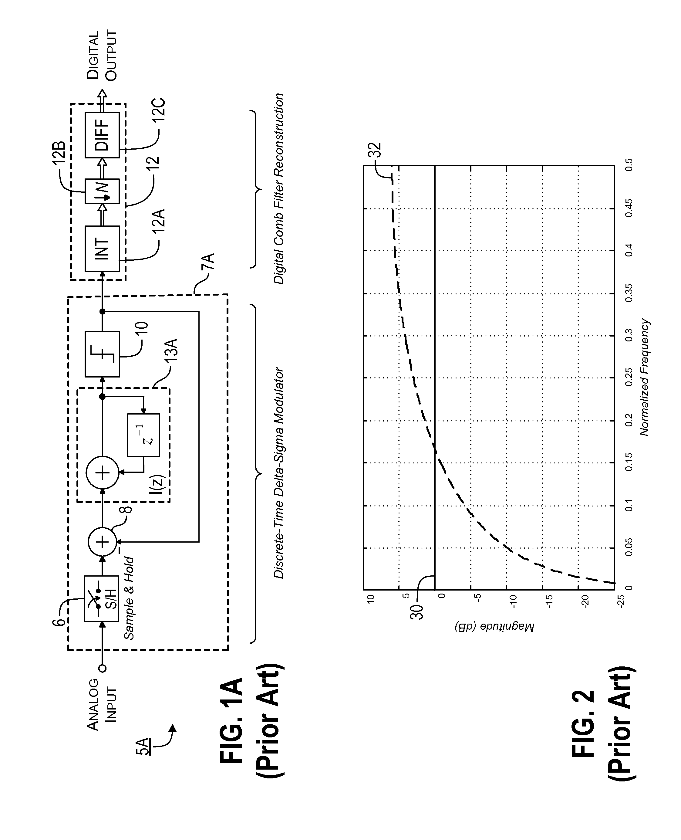
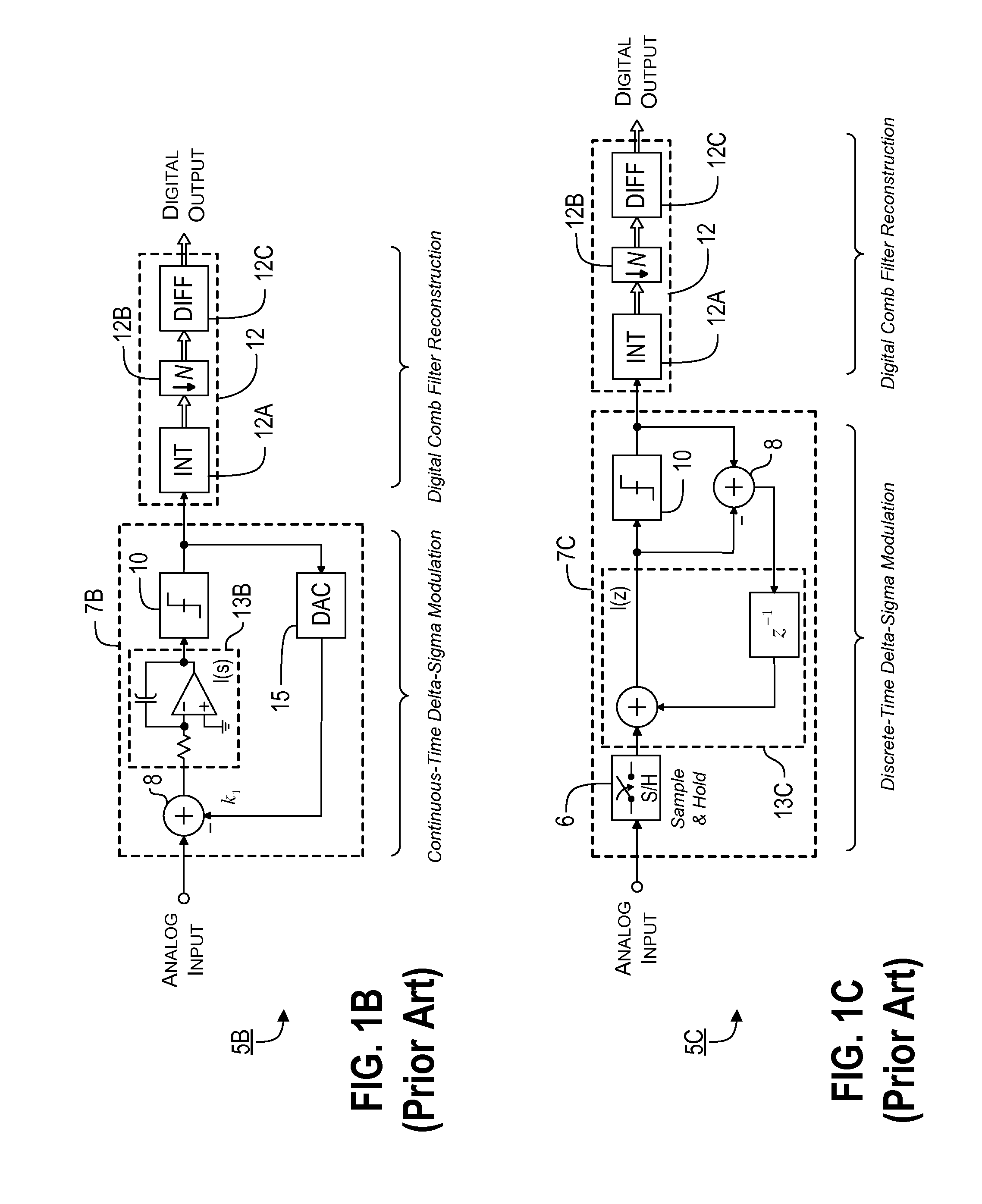
n; FIGS. 14C-E are block diagrams illustrating representative forms of recursive moving average prototype filters for BMA signal reconstruction; and FIG. 14F is a simplified block diagram of a multirate, recursive moving average filter having a polyphase decomposition factor of m=4.

[0036]FIG. 15A illustrates frequency responses of a Bandpass Moving Average signal reconstruction filter bank used in a MBO converter according to a representative embodiment of the present invention; and FIG. 15B illustrates the frequency responses of a conventional signal reconstruction FIR filter bank based on a Kaiser window function.

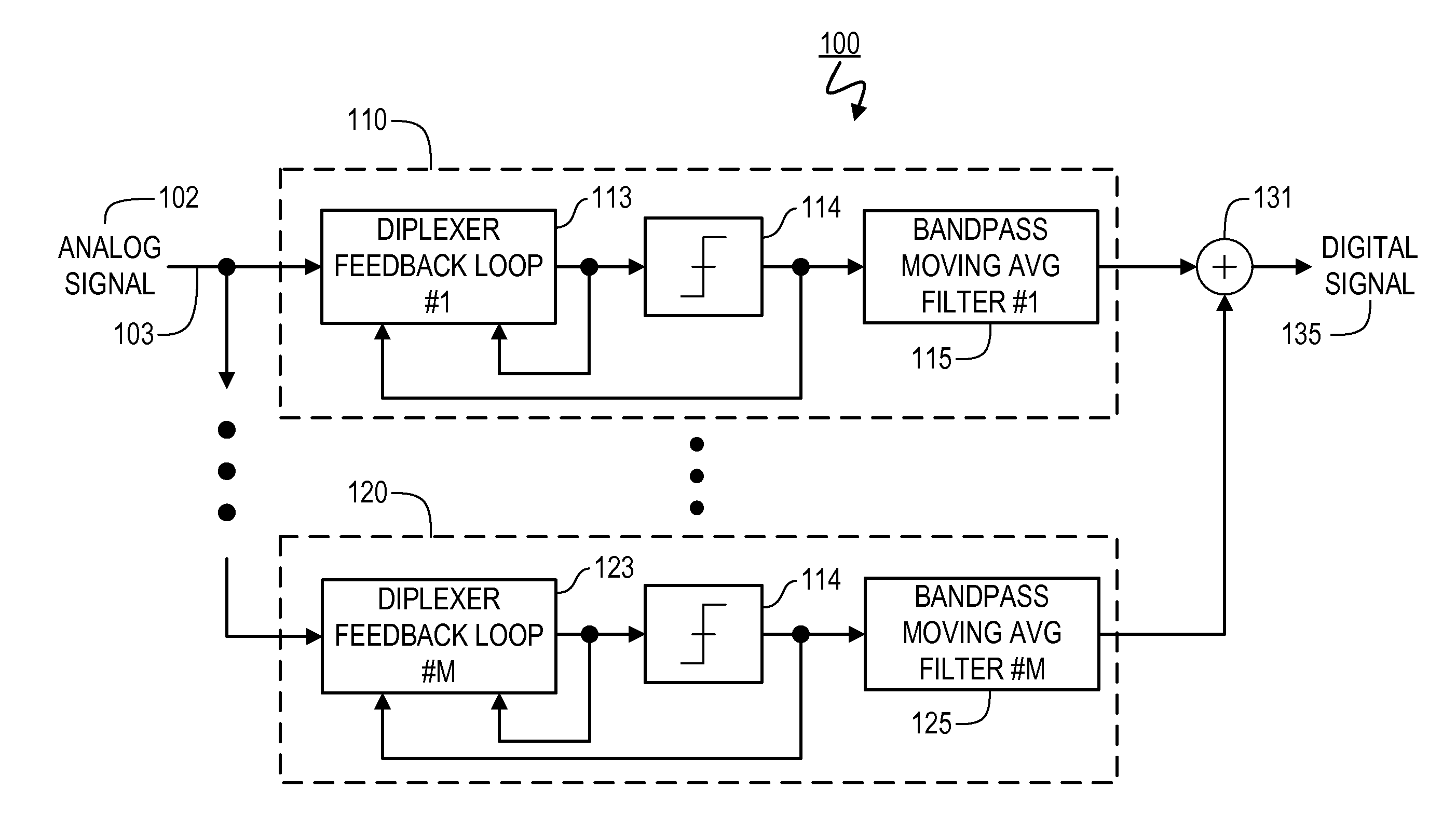
[0037]FIG. 16 is a block diagram of a complete MBO converter according to a representative embodiment of the present invention, which incorporates multiple Diplexer Feedback Loop (DFL) noise shaping circuits in conjunction with a Bandpass Moving Average (BMA) filter bank for signal reconstruction.

[0038]FIG. 17 is a block diagram of a complete MBO converter according to a ...


PUM


Abstract

Provided are, among other things, systems, methods and techniques for converting a continuous-time, continuously variable signal into a sampled and quantized signal. According to one representative embodiment, an apparatus includes multiple continuous-time quantization-noise-shaping circuits, each in a separate processing branch and having an adder that includes multiple inputs and an output; an input signal is coupled to one of the inputs of the adder; the output of the adder is coupled to one of the inputs of the adder through a first filter; and the output of a sampling / quantization circuit in the same processing branch is coupled to one of the inputs of the adder through a second filter, with the second filter having a different transfer function than the first filter.

Description

[0001]This application is a continuation in part of U.S. patent application Ser. No. 12 / 824,171, filed on Jun. 26, 2010 and titled “Sampling / Quantization Converters” which, in turn, claimed the benefit of U.S. Provisional Patent Application Ser. No. 61 / 221,009, filed on Jun. 26, 2009, and titled “Method of Linear to Discrete Signal Transformation using Orthogonal Bandpass Oversampling (OBO)” and U.S. Provisional Patent Application Ser. No. 61 / 290,817, filed on Dec. 29, 2009, and titled “Sampling / Quantization Converters”. The present application also claims the benefit of: U.S. Provisional Patent Application Ser. No. 61 / 414,413, filed on Nov. 16, 2010, and titled “Sampling / Quantization Converters”; U.S. Provisional Patent Application Ser. No. 61 / 381,055 (the '055 Application), filed on, filed on Sep. 8, 2010, and titled “Multi-Bit Sampling and Quantizing Circuit”; and U.S. Provisional Patent Application Ser. No. 61 / 292,428, filed on Jan. 5, 2010, and titled “Method and Apparatus for ...

Claims


Application Information

Patent Timeline
Patent Type & Authority Applications(United States)
IPC IPC(8): H03M1/50
CPCH03M3/414H03M3/468H03M3/436H03M3/422
Inventor PAGNANELLI, CHRISTOPHER
Owner PAGNANELLI FAMILY TRUST
Learn More