Scalable thermally efficient pump diode assemblies
a technology of pump diodes and diodes, applied in electrical devices, semiconductor lasers, laser details, etc., can solve the problems of large energy loss, subject to various undesirable effects, and significant energy loss, and achieve the effect of improving heat removal and more efficient excitation of the medium
- Summary
- Abstract
- Description
- Claims
- Application Information
AI Technical Summary
Benefits of technology
Problems solved by technology
Method used
Image
Examples
example 1
Pump Diode Assembly with at Least One Emitter
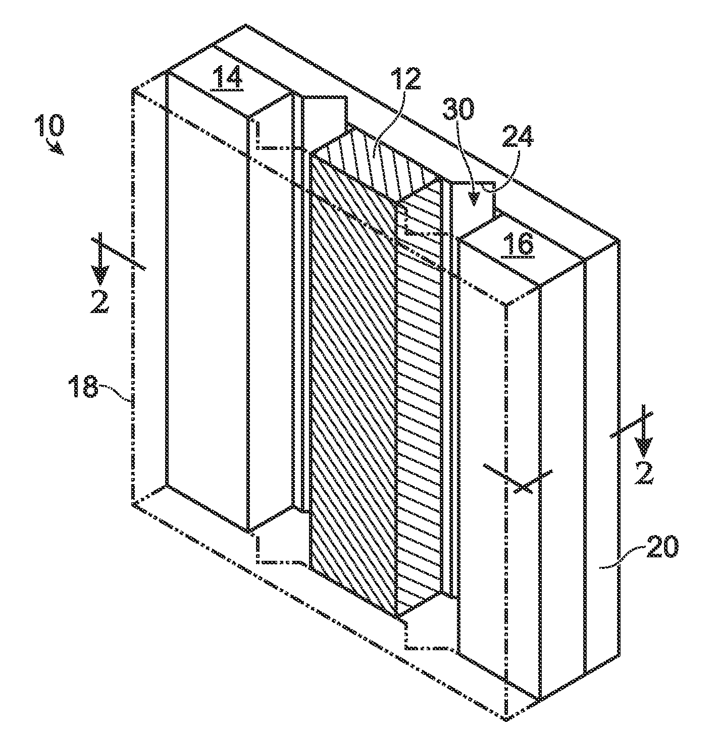
[0043]This example describes an exemplary pump diode assembly 10 having at least one emitter, in accordance with aspects of the present disclosure; see FIGS. 1 and 2. The pictured embodiment includes one emitter and two spacers. However, in other embodiments, one or both spacers may be replaced by additional emitters to increase the fill factor of the diode assembly. Yet other embodiments may include larger numbers of emitters and / or spacers (see, for example, Examples 3 and 5).
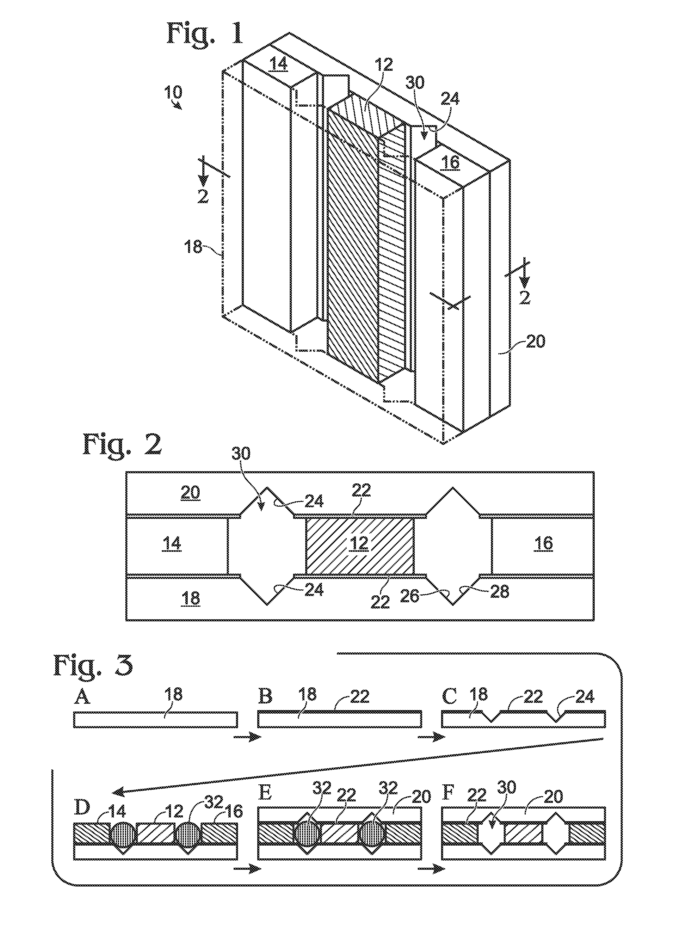
[0044]FIGS. 1 and 2 show diode assembly 10 in isometric and cross-sectional views, respectively. Diode assembly 10 includes one emitter 12, two spacers 14, 16, and first and second substrates 18, 20, configured such that the emitter and spacers are sandwiched between, and at least partially supported by, the first and second substrates. Conductive layers 22 (visible in FIG. 2) may be disposed adjacent the first and second substrates (in particular, between each sub...
example 2
Method of Manufacturing a Pump Diode Assembly
[0051]This example describes an exemplary method for manufacturing a pump diode assembly, such as the pump diode assembly of FIG. 1, in accordance with aspects of the present disclosure; see FIG. 3.
[0052]FIG. 3 shows an exemplary series of configurations (Panels A-F) produced during manufacture of the pump emitter assembly of FIG. 1. For clarity, and to emphasize the emitter, substrates and spacers are shown without hatching.
[0053]Panel A. A substrate 18 is obtained.
[0054]Panel B. A conductive layer 22 is applied to a surface of substrate 18, using any suitable method. For example, the conductive layer may be applied using chemical vapor deposition (CVD), among others. The surface(s) receiving the conductive layer may include, or be limited to, surfaces that will contact emitters and / or spacers.
[0055]Panel C. A plurality of grooves 24 is formed through conductive layer 22 and, optionally, partially through first substrate 18, using any su...
example 3
Pump Diode Assemblies with a Linear One-Dimensional Array
[0060]This example describes exemplary pump diode assemblies having linear one-dimensional arrays of N emitters, in accordance with aspects of the present disclosure; see FIGS. 4 and 5. The number N of emitters may be selected according to any suitable criteria, such as intended use. Exemplary numbers may include 2, 3, 5, 10 (as shown), 15, 20, or more, among others. Power may be supplied to the emitters using any suitable mechanism(s), including series (e.g., FIG. 4), parallel (e.g., FIG. 5), and / or a combination thereof (e.g., parallel across adjacent pairs of emitters and in series across adjacent pairs of pairs of emitters, among others).
[0061]Series Embodiment
[0062]FIG. 4 shows a cross-sectional view of a linear pump diode assembly 50 of ten (10) single emitters, or emitters, connected in series, in accordance with aspects of the present disclosure.
[0063]Pump diode assembly 50 includes a plurality of emitters 52 between a...
PUM
 Abstract
Description
Claims
Application Information
 - R&D
- Intellectual Property
- Life Sciences
- Materials
- Tech Scout
- Unparalleled Data Quality
- Higher Quality Content
- 60% Fewer Hallucinations
Browse by: Latest US Patents, China's latest patents, Technical Efficacy Thesaurus, Application Domain, Technology Topic, Popular Technical Reports.
© 2025 PatSnap. All rights reserved.Legal|Privacy policy|Modern Slavery Act Transparency Statement|Sitemap|About US| Contact US: help@patsnap.com


